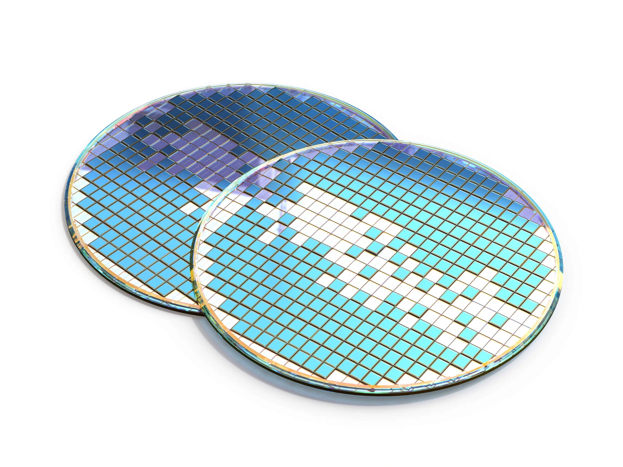
Understanding intrinsic carrier concentration is fundamental to mastering silicon wafer manufacturing. Whether you’re fabricating power semiconductors, solar cells, or advanced sensors, carrier concentration determines how pure silicon behaves electrically—and how precisely you can control its performance.

Intrinsic carrier concentration, typically denoted as ni, represents the number of electrons and holes generated in pure silicon at thermal equilibrium. Unlike doped silicon, intrinsic material has no intentional impurities; its conductivity comes solely from thermal excitation.
In wafer production, this parameter influences resistivity, leakage current, and overall device stability. Precise control over ni helps manufacturers fine-tune doping levels, ensure consistency between wafers, and maintain tight process windows for advanced nodes.
At room temperature (approximately 300 K), silicon has approximately 1.1 × 10^10 carriers per cubic centimeter (cm^-3). This value denotes the number of free electrons and holes in pure silicon at this temperature.
These values are essential for wafer simulation, doping calibration, and yield optimization. Even minor temperature deviations during Czochralski crystal growth or diffusion processing can shift intrinsic concentrations, impacting uniformity and defect density.
By understanding silicon’s intrinsic carrier concentration, you can gain a competitive edge. Correlating intrinsic carrier variation with temperature and defect analysis can minimize yield loss, predict resistivity drift, and enhance wafer-to-wafer consistency.
In short: mastering intrinsic carrier concentration is key to manufacturing next-generation electronics. Would you like to learn more about our product’s specs? Contact Wafer World today for more information!


