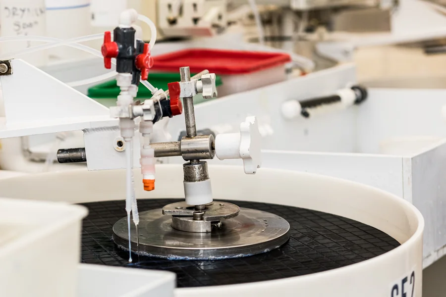
Every phone, car sensor, and data center rack traces back to a thin, gray disc that started life as common beach sand. That disc is a single wafer, and the distance between raw silica and a finished, mirror-polished substrate involves more precision than most buyers ever stop to consider.
Before diving into specs and sourcing decisions, it helps to browse the full product catalog to see just how many variations of this one material actually exist.
Silicon is the second most abundant element in the Earth's crust. Yet the sand on a beach is nowhere near suitable for chip production. According to the Semiconductor Industry Association, raw silica first undergoes carbothermic reduction to produce metallurgical-grade silicon, which is only about 98% pure and lacks a well-defined crystal structure.
From there, a further refinement called the Siemens process converts it into electronic-grade polysilicon, purified to at least eleven nines, or 99.999999999%. That level of purity is not a marketing number. It is a baseline requirement before the material can even be considered for wafer production, since a single stray metallic atom can disrupt an entire circuit's electrical behavior.
Once that ultra-pure polysilicon exists, it still has to become a single, perfectly aligned crystal. Manufacturers typically rely on the Czochralski method, pulling a seed crystal from a molten silicon bath to grow a cylindrical ingot with uniform atomic alignment throughout. This ingot is eventually sliced into wafers that reach the fabrication floor.
Purity alone does not make silicon useful for electronics. Pure silicon is actually a poor conductor, which is why manufacturers introduce controlled impurities, a process called doping, to give the material specific electrical properties. Adding elements like phosphorus creates an n-type wafer with extra free electrons, while boron produces a p-type wafer with electron vacancies, or holes, that also conduct current. The ratio and placement of these dopants determine resistivity, which in turn determines how a chip built on that wafer will behave once it is powered on.
This is why two wafers that look identical under normal lighting can perform completely differently in a finished device. A wafer destined for a power transistor needs a different doping profile than one destined for a memory chip, and getting that wrong cannot be corrected later in the process. A properly specified Si wafer arrives with its resistivity, orientation, and dopant type documented in detail, so the fab receiving it already knows exactly how it will behave under load.
Our wafer services team works through these specifications with engineers before a single ingot is cut, which saves both sides from expensive rework once production begins.
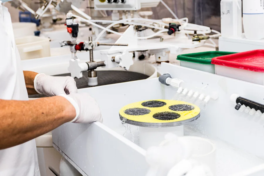
After the ingot is sliced, the individual discs are dull gray and rough to the touch. Getting them to a usable state involves several distinct mechanical stages, each one addressing a different structural weakness left over from cutting.
Skipping or rushing any of these steps shows up later as yield loss on the customer's fab line, which is a far more expensive problem than a slightly longer lead time up front.
The global silicon wafer market is no longer a niche corner of manufacturing. Industry estimates put annual global silicon wafer purchases at roughly 13.5 billion dollars, with projected growth to 18.3 billion dollars by 2029, a compound annual growth rate near 6.4%. That growth is being driven by artificial intelligence hardware, automotive electronics, and the steady expansion of connected devices, all of which require substrates that meet increasingly tight specifications.
Anyone sourcing wafers today is competing for capacity with some of the world's largest chipmakers, making supplier relationships and specification accuracy more important than ever. Smaller labs, universities, and startups working on prototype hardware often find themselves squeezed out of standard supply chains that prioritize massive volume orders. Working with a supplier that also serves smaller batch sizes and custom specifications, rather than only bulk production runs, tends to matter more to these teams than headline pricing ever will.
It is worth checking a supplier's company background before committing to a long-term sourcing relationship, since track record and accreditation say more about reliability than a catalog page ever can.
Not every project requires a brand-new, prime-grade wafer straight off the line. Test runs, process qualification, and certain research applications can often be handled just as effectively with a reclaimed wafer, which has been stripped of prior films and reprocessed back to a usable surface at a lower cost.
Our silicon reclaim program is designed specifically for teams that want to control costs without compromising the consistency their process requires. Once wafers are ready to ship, they also pass through our cleanroom packaging process to eliminate the risk of contamination entirely.
A wafer is the raw substrate. A chip, or die, is what remains after a wafer has undergone lithography, etching, and packaging inside a fabrication facility.
No. Common sizes range from 25.4 millimeters to 300 millimeters, with larger diameters generally favored for high-volume production since more chips can be cut from a single wafer.
Yes, provided the reclaiming supplier has proper stripping, polishing, and inspection procedures in place. A properly reclaimed wafer can perform reliably for test and qualification purposes.
Doping changes the material's electrical behavior at the atomic level, which is invisible to the naked eye but critical to how the finished chip conducts current.
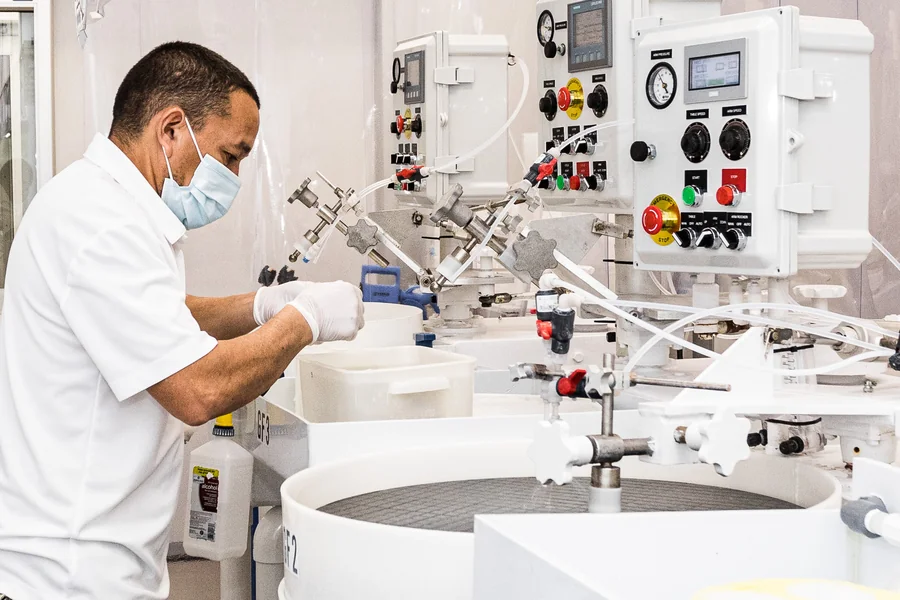
Choosing a Si wafer is not a decision to make on price alone, since purity, doping accuracy, and surface finish all affect whether a finished device performs as designed. Our team at Wafer World has spent years refining every stage of that process, from ingot growth through final inspection, so that engineers and procurement teams can order with confidence rather than guesswork.
If you are ready to discuss specifications for your next batch or want guidance on choosing between prime and reclaimed materials, contact us and we will help you find the right fit for your application.




