When it comes to wafer manufacturing, it’s not just a one size fits all type of scenario. There are many different types of wafers that are made for multiple different reasons. They each have their own unique properties and characteristics which separate them from the others, so it’s best to have an idea regarding which wafer is best for you when you’re ready to make a purchase from a silicon wafer supplier. For example, a reclaimed wafer might be used for testing because they are cleaned and reprocessed so they can be repurposed. On the other hand, there’s the double side polish wafer, which is known for its flatness and is used for microelectromechanical systems and wafer bonding. Each need for a wafer has a one that’s the best fit for that task. You may even a choice between a more expensive or cost-effective choice. It’s important to find a balance between those two. Whatever the reason for your wafer needs, we have a guide of some of the most common types of wafers on the market, so you know which type would be the most effective for your project. https://youtu.be/yCRfPGapFR0
InP wafers are typically used for electronics requiring a high frequency and a lot of power. InP stands for indium phosphide, which is a binary semiconductor made from a combination of indium and phosphorus. If you’re looking for a higher electron velocity, radiation resistance, and good thermal conductivity, this is a great choice compared to some of your other options. Some of the most common applications include:
Optoelectronics includes technology that emits or detects light. Devices that emit light produce electromagnetic radiation through the use of voltage and currents, while devices that detect light take electromagnetic energy and convert it into an electric current or voltage. Examples of this would be security systems, infrared detectors, and lighting control.
Another common use for InP wafers is telecommunications due to its ability to convert laser signals into electronic form. This means they’re great for applications such as wireless connections, satellites, and networks.

InP reclaim wafers are very similar to normal InP wafers other than their thickness. The reclaim wafers are a little bit thinner, meaning a slightly different performance level, but since these are typically used for testing purposes, it shouldn’t be enough of a difference to be an issue. Reclaimed wafers are cleaned and reprocessed in order to be repurposed, meaning they are a more inexpensive alternative, making them perfect for those testing reasons. This can actually be completed multiple times until the wafer becomes too thin.
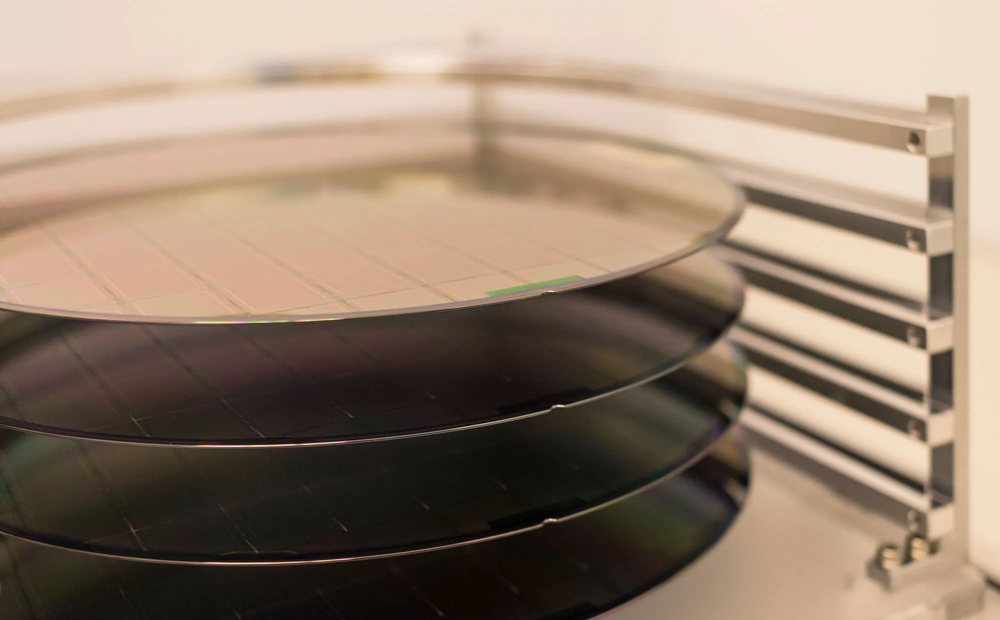
A double side polish wafer is known for its flatness, which is accomplished by polishing both sides. This not only improves flatness, but it also creates a mirror-like surface that’s both defect-free and uncontaminated. These wafers are of extremely high quality and are used for products where flatness is a necessary characteristic.

The float zone wafer method from Henry Theuerer differs from the Czochralski method due to the low concentration of both carbon and oxygen. This is accomplished by having the complete manufacturing process take place under a vacuum, resulting in an extremely pure silicon wafer that has higher resistivity. Wafers manufactured through the other method contain oxygen that will ultimately reduce functions such as the voltage, current, and efficiency, plus make them more susceptible to being affected by higher temperatures. Due to their unique characteristics, these float zone wafers are commonly used for solar products and optical applications.
GaAs wafers are composed of gallium arsenide and are an alternative to the more traditional silicon wafer semiconductors. While silicon is going to be your more cost-effective option when purchasing from a wafer supplier, GaAs wafers have their own advantages that set them apart from the rest, which makes them perfect for radar and solar cells. Some main benefits of using GaAs wafers over the traditional silicon ones include their high thermal stability, high saturated electron velocity, and high electron mobility. Due to its wide direct bandgap, they are also the perfect wafers necessary for electronics meant to be used for applications in outer space.
Just like how InP wafers can be reclaimed, the same can be done for GaAs wafers, meaning they can be stripped, polished, and cleaned so they can be repurposed. Since GaAs wafers are typically the more expensive option in the first place, using reclaimed wafers for testing can save you a lot of money than deciding to go with brand-new wafers.

Germanium wafers are mainly known for their crystallographic and electric properties and are another alternative option to the more widely used silicon wafers. In order to create them, germanium is transformed into a crystal through the Czochralski process. That crystal is then cut and etched into a wafer before being cleaned and inspected. During this stage, the wafer is polished on either one or both sides depending and what it will be used for. These wafers are very light while still being strong, making them a good choice for multiple projects. Some of the most common uses of germanium wafers include:
Ultra flat wafers extremely thin – less than 200 microns. While these are often double side polished, they are also available as a single side polished wafer. Their size makes them the perfect choice for micro-fabrication applications or any other situation that calls for filling up less space. Plus, due to their low background signal, they are also very useful for high-resolution SEM imaging.

When you come to Wafer World for your needs, know that we strive to be the very best silicon wafer supplier you can find. We have a wide selection of wafers, such as silicon, germanium, and float zone, plus we have a quality manufacturing process so that you only receive the very best. If you have a need for it, we can help. If you have any questions or if you’re ready to make a purchase, contact us today for inquiries!


