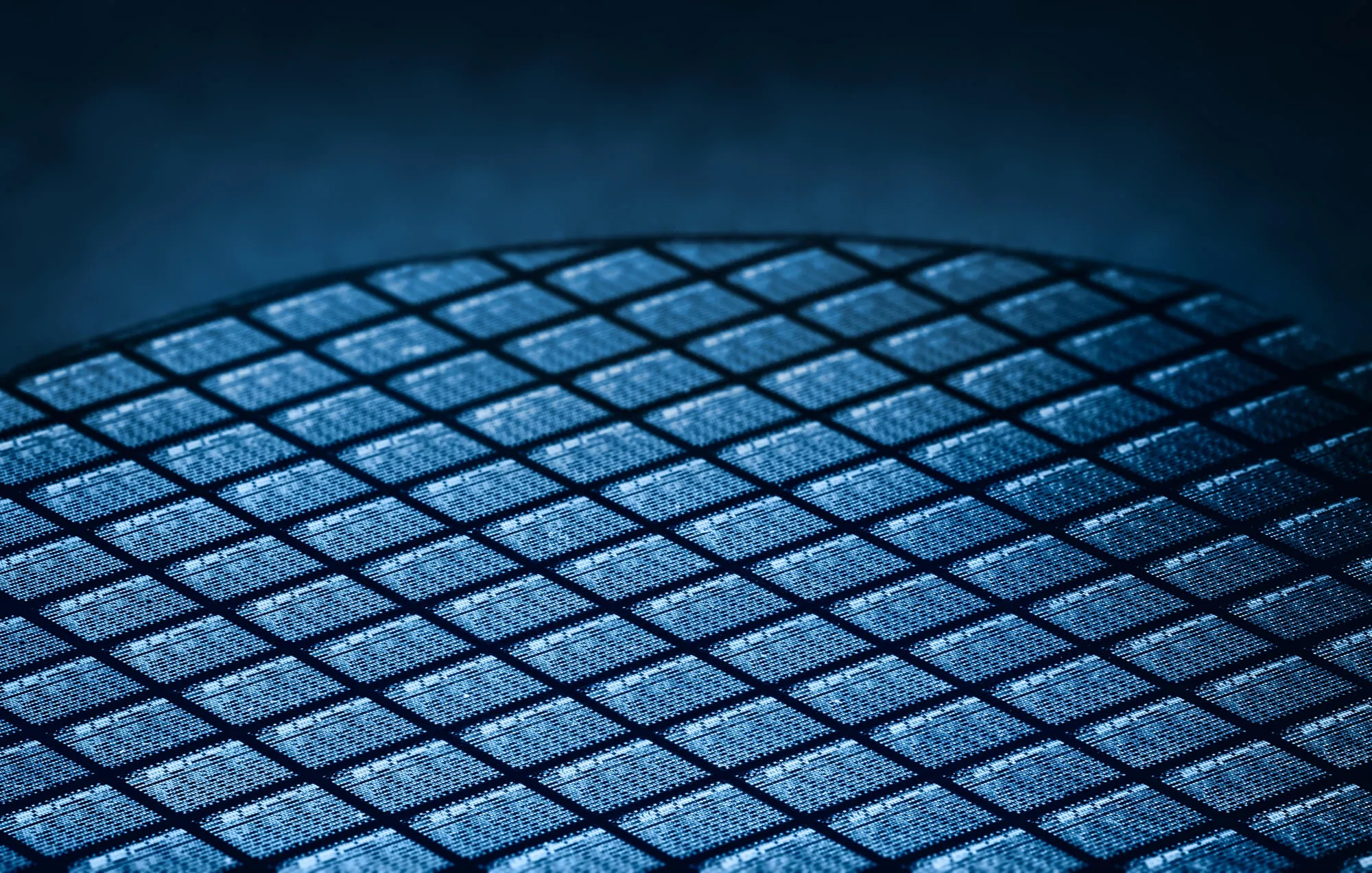
Silicon wafers come in different shapes, sizes, and uses. One example is doped silicon wafers which are currently gaining much attention among silicon wafer suppliers. A highly doped silicon wafer is used when a semiconductor or electrical device needs to be heavily doped.
For many applications, a highly doped wafer is a fantastic material option. If you want to learn more about this material, here are all the facts that you need to know about this type of silicon wafer.
https://www.youtube.com/watch?v=nNxbWcNgF2s&ab_channel=WaferWorldInc.
A silicon wafer with an added element is a doped silicon wafer. To produce positive or negative charges, the silicon wafer can be doped with either P-type or N-type silicon. Boron, phosphorus, arsenic, and antimony are just a few impurities that can be added when doping is carried out during the formation process.
A doped silicon wafer's primary function is to facilitate energy flow by lowering resistance and making non-doped material more conducive to current flow. Electronics and solar cells frequently employ doped silicon to help regulate the electricity flow.
Wafers with unusual shapes are created using doped silicon. These wafers are made by coating a silicon wafer with an oxide underneath and a thin layer of aluminum oxide if a bit of silicon is heated for about five minutes at 900 °C in an oxygen-rich environment.
Due to the defects created during the silicon manufacturing process, silicon can be used as a heating source. The peculiarity of doped silicon wafers is that they contain one or more "dopant atoms." Hydrogen or boron atoms have been added to improve the properties of the aluminum oxide layer that is layered on top of the silicon substrate.
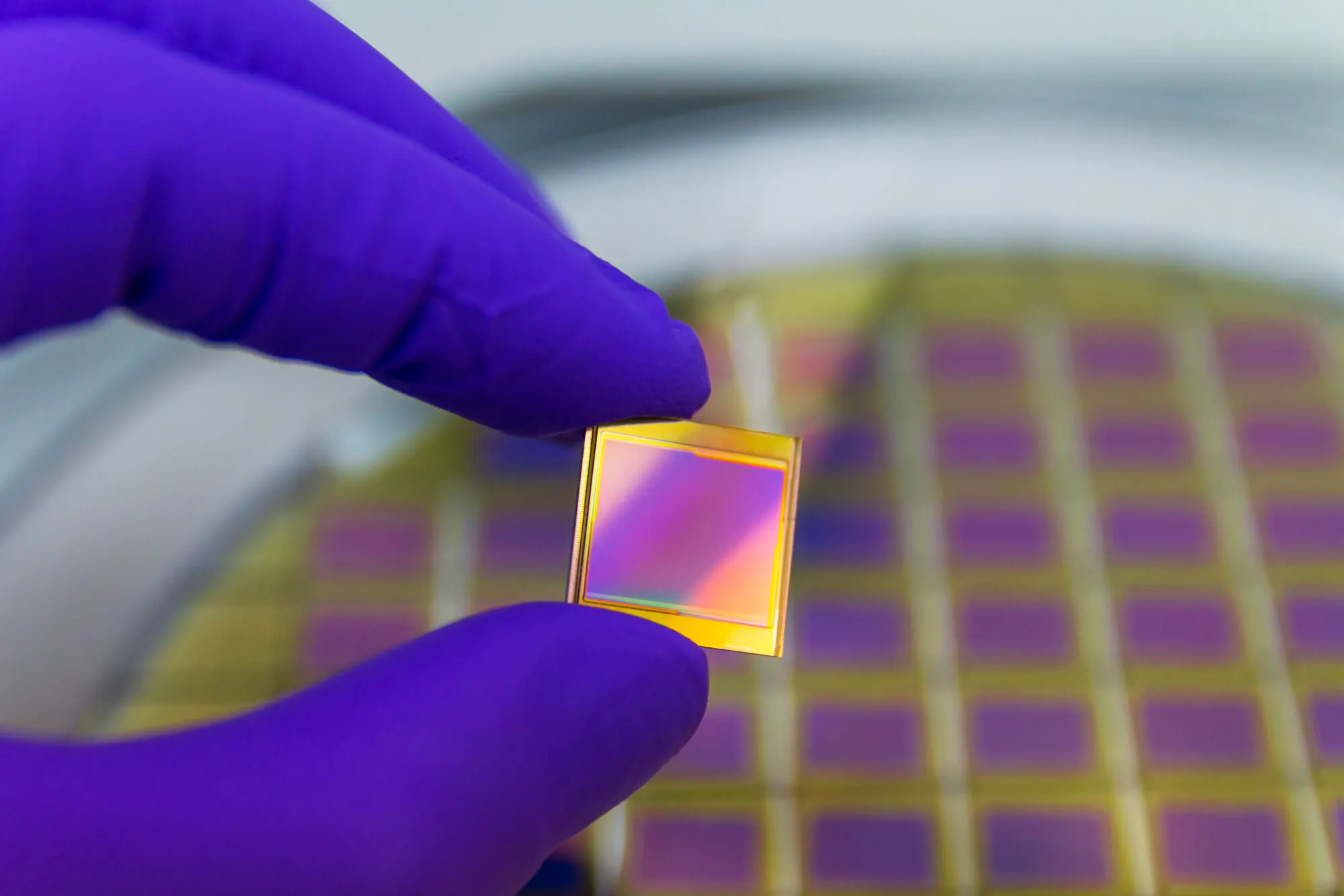
These substances are semiconductors and can function as insulators or conductors when electricity passes through them. For instance, light detectors and photovoltaic solar cells are made of doped semiconductors implanted with silicon dioxide wafers. These materials also create doped silicon wafers in various applications besides solar cells.
The substances used to alter the material's conductivity can be used to categorize these doped silicon wafers. Boron is used in type I wafers, and hydrogen in type II wafers. Type III wafers have a doping profile between Type I and Type II. Type III wafers typically have properties that fall somewhere between Type I and Type II characteristics.
In today's electronics, doped semiconductors increase the devices' efficiency and power compared to those made of undoped semiconductors. It is best if the dopant is evenly distributed throughout the silicon wafers during the manufacturing process. Silicon wafers can contain a wide variety of dopants which adds to the efficiency of semiconductors.
Doped silicon wafers are sometimes used to decrease the number of free electrons in the wafer and turn silicon semiconductors into metallic conductors.
Transistors, diodes, and integrated circuits are made from doped semiconductors. Doped semiconductors can enhance several electronic properties of components, such as transistors, which form the circuitry in computers and other electronic devices.
The consensus is that silicon wafers with higher doping levels are more brittle than those with lower doping levels. It is typical for silicon crystals to break easily under certain stress conditions because they frequently clump together during heating. Thermal expansion and compressive stresses brought on by weight transfer when using a transducer are the causes of these stresses.
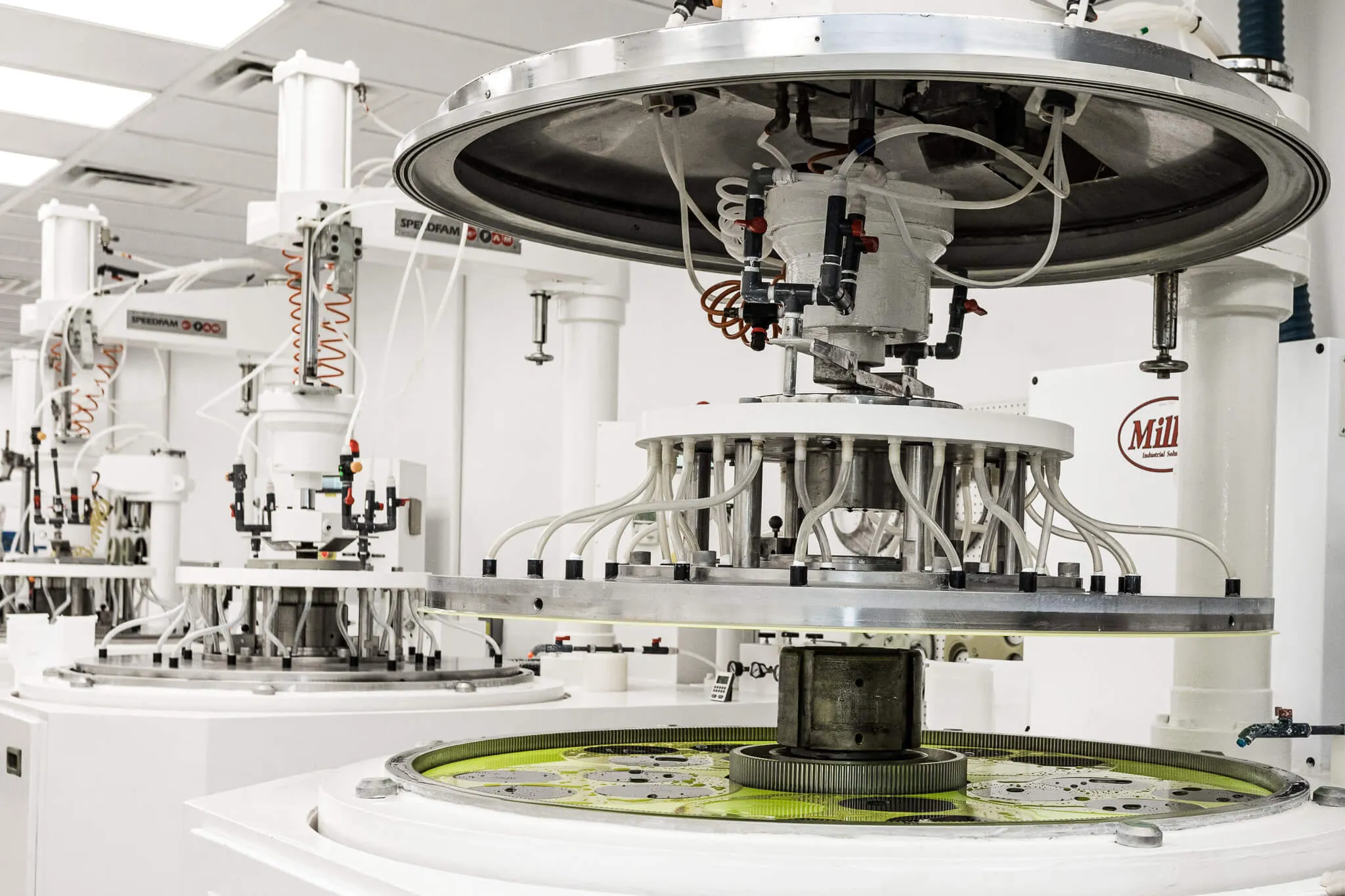
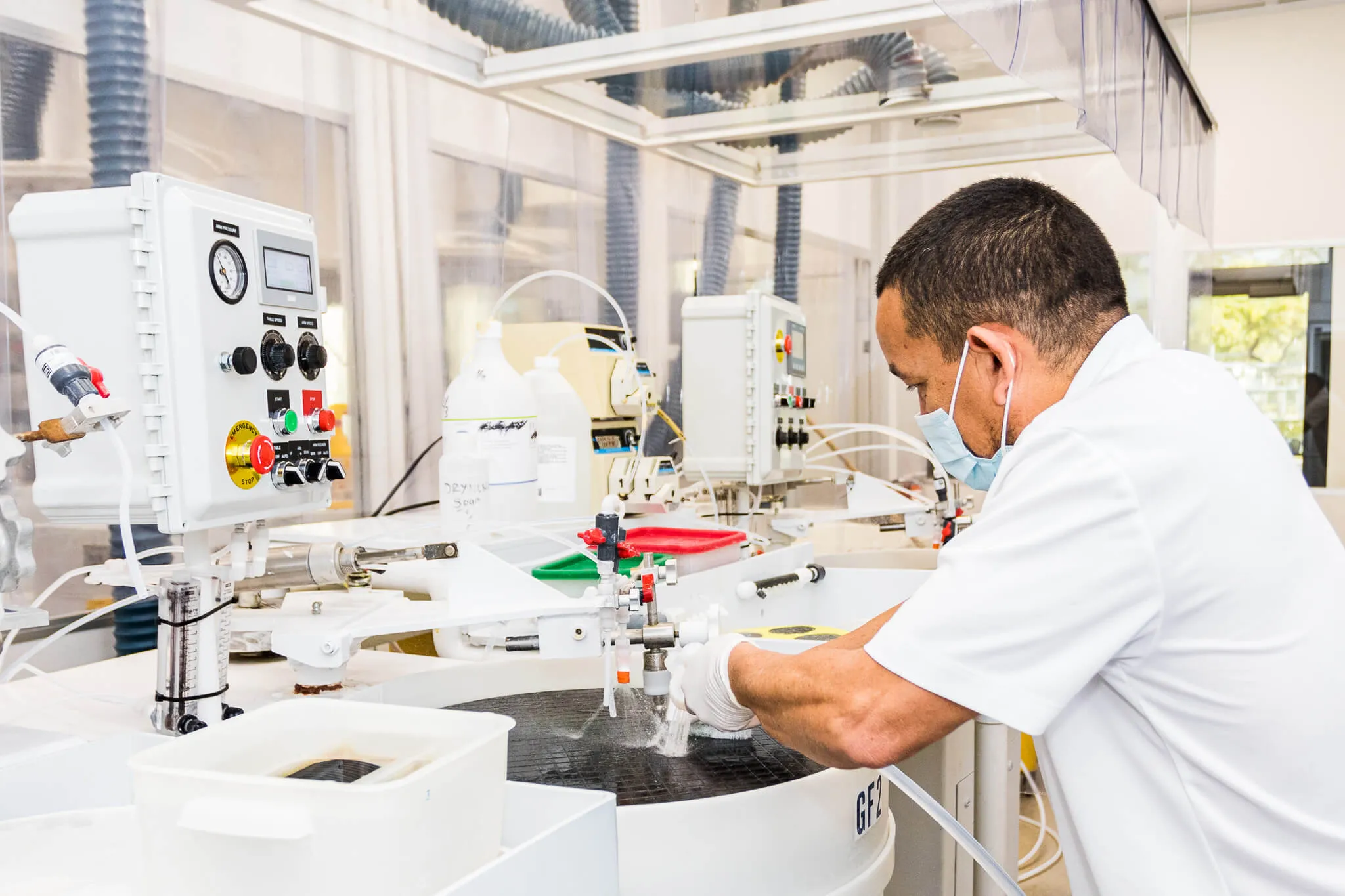
The highly-doped silicon wafers are frequently made by subjecting them to high pressures and temperatures, then shaping them into a smooth surface that resembles silica, which is used in numerous microelectronic applications.
The thermal conductivity of highly-doped silicon wafers is one exciting development in the photo-electric microscopy field that has occurred recently. Due to the tightly packed crystalline structure in the wafer structure, High-Performance Silicon (HPOS) has excellent thermal conductivity. We can conduct electric currents through the crystalline structure of HPOS by generating an electrical field.
This technique not only differs from most other methods in photo-electric microscopy, but it also enables us to watch electron transfer between adjacent crystalline structures.
For years, vacuum tubes, desiccant tubes, electrical insulators, gas detectors, gyrostagens, and thermal conductors were made using highly-doped silicon carbide wafers. Mechanical parts like bearings, valve seats, pawls, shaft seals, lock pins, hinges, bearing housings, cam locks, spring retainers, and knobs were also made from it. This substance was also used to create electronic components because of its numerous uses.
Making highly doped silicon wafers requires a lot of processes, including hardening processes. The heat hardened the wafer during this process, enabling its use in subsequent applications. It allows the production of wafer sheets with significantly better electronic properties than regular solid silica sheets. This property enables highly doped sheets to transmit data at a higher bandwidth and use less power.
The crystalline structure is then prevented from collapsing by spraying cure urethane onto the fine aluminum oxide layer. The wafer is then put inside a spinning machine, which is subjected to scanning electromagnetic energy after this spraying.
The radiation output is strongly influenced by the scanning frequency and depends on the thickness of the highly-doped wafer. After passing through the highly doped wafer, the energy flow produces a positively radiant field that excites the wafer's electrons.
The working chamber's temperature must be maintained at about 300 degrees Celsius when silicon carbide creates highly doped silicon wafers. This will stop bubbles from forming during scanning or electron micrographic processes. The crystalline structure will collapse if the temperature is allowed to increase above this, shortening the useful life of the highly-doped wafer.
Another way to stop bubbles from forming while scanning is to use a vapor-gas control to regulate the temperature. The surface of the semiconductor is first prepared by grinding to create highly-doped silicon wafers. The aluminum oxide then forms a fine mesh on the surface. Plasma cutting is a method used to develop silicon carbide wafers.
At Wafer World, our team can supply your business with high-quality wafers. To learn more about our different materials, give us a call today!


