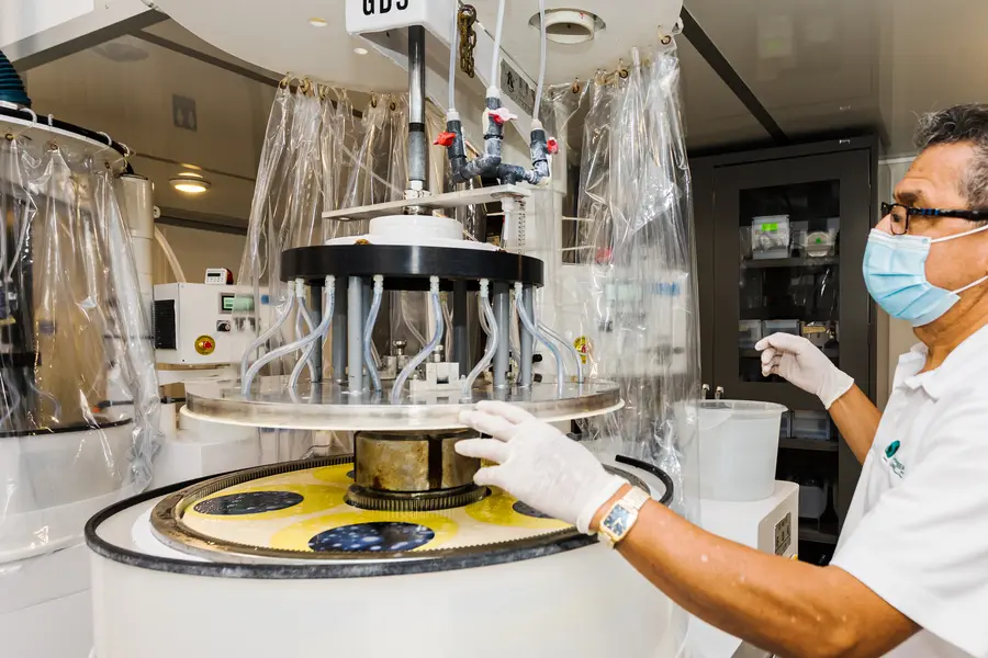
A modern chip has features measured in nanometers, smaller than most airborne dust by a wide margin. That mismatch in scale is exactly why a single stray particle, invisible to the eye, can ruin a wafer partway through wafer manufacturing without anyone noticing until testing catches the defect.
Our earlier look at the clean room protocol covers the basics of how that risk is managed. Still, the more specific question is which cleanroom class applies to each step.
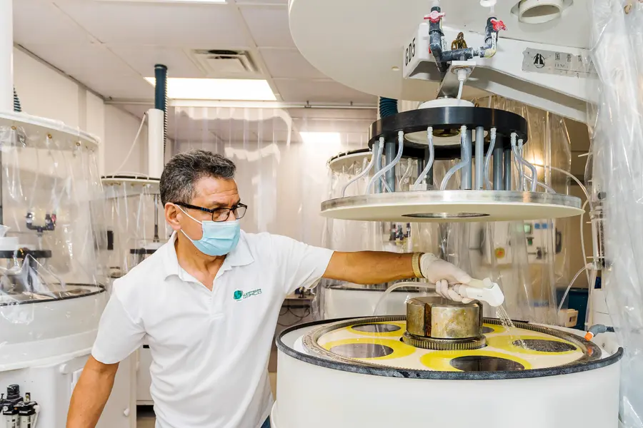
Not every part of a facility requires the same level of cleanliness, and treating the entire building as a single uniform cleanroom would be needlessly expensive. According to TSI, a manufacturer of cleanroom monitoring instruments, semiconductor facilities typically operate across several ISO 14644 classes depending on the process step involved.
Matching the class to the step matters because over-specifying cleanliness everywhere adds enormous cost without adding meaningful protection where it is not needed, while under-specifying it in the wrong zone creates real yield risk.
The particle sizes that matter shrink as the process advances, which is part of why a facility built for older technology cannot always support newer, more sensitive wafer manufacturing without significant upgrades.
Packaging carries its own separate cleanliness requirement rather than inheriting whatever class the fabrication area used. Our own clean room packaging service typically operates in ISO Class 3 or Class 4 environments specifically to keep finished wafers contaminant-free between fabrication and shipment, since a clean wafer can still pick up particles during handling if packaging is not held to a comparable standard.
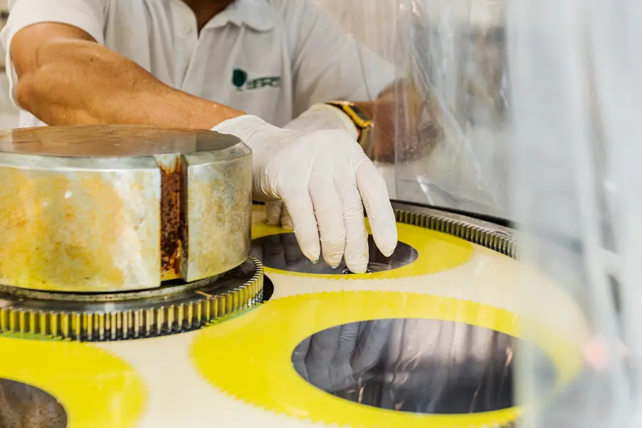
Class-appropriate cleanrooms, documented protocols, and consistent handling standards all contribute to whether a batch actually meets specification upon arrival. Request a quote from Wafer World and ask directly about the contamination controls behind your wafer manufacturing order.




