
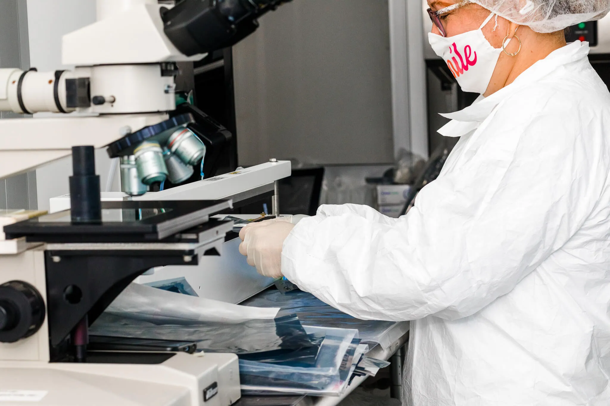
As consumer demand drives the semiconductor industry toward ever smaller, faster, and more powerful chips, silicon wafer manufacturers face increasing pressure to keep pace. One of the most critical breakthroughs enabling this evolution is EUV lithography—a cutting-edge process revolutionizing how next-generation semiconductors are made.

EUV (Extreme Ultraviolet) lithography is an advanced photolithography technique for patterning incredibly small features on silicon wafers. Unlike traditional deep ultraviolet (DUV) lithography, which uses 193 nm light, EUV operates at a wavelength of just 13.5 nanometers.
This shorter wavelength allows manufacturers to etch finer circuit patterns, essential for producing chips at sub-7nm nodes and beyond.
The technology relies on high-powered lasers to generate EUV light, which is then directed through a complex system of mirrors (not lenses, as EUV light is absorbed by glass) to project patterns onto photoresist-coated wafers.
EUV lithography allows silicon wafer manufacturers to:
EUV lithography offers several advantages for silicon wafer manufacturers. However, adoption of this new technology remains slow, and it’s not hard to figure out why: A single EUV scanner from ASML can cost over $150 million.
At Wafer World, we’re attentive to what’s to come in the semiconductor industry. To stay up-to-date with new technologies and news, contact us today!


