Reducing wafer thickness can enable advanced packaging and other applications where compact dimensions are important, but removing silicon imposes tighter manufacturing requirements. With thin silicon wafers, manufacturers must control not only the target thickness but also the consistency with which that thickness is maintained across the substrate. Small variations can become increasingly significant as the remaining material becomes thinner.
Mechanical back-grinding is an established method for reducing wafer thickness. The International Technology Roadmap for Semiconductors identifies silicon thickness control and surface quality as critical considerations in wafer thinning, particularly for through-silicon via technology.
The grinding process must remove sufficient material to achieve the specified thickness without causing unacceptable variation. This makes equipment accuracy and process control important throughout thinning rather than only at final inspection.
A single thickness reading cannot describe the entire wafer. Total thickness variation, or TTV, reflects the difference between thicker and thinner areas across a measured wafer.
According to the semiconductor technology roadmap, TTV in a thinned wafer can be influenced by several factors in the thinning setup, including the carrier wafer, temporary adhesive layer, and grinding tool accuracy. Therefore, controlling the final result requires attention to the complete process stack.
Silicon is a brittle material, so thinner substrates require thoughtful handling. NIST research evaluating packaging for 50 µm and 100 µm silicon substrates found that some samples fractured during drop testing, with significant edge defects associated with the observed failures.
Several considerations become especially important during production:
Thickness control is therefore connected to more than dimensional compliance. It also fits into a larger strategy for safely processing and moving fragile substrates.
Mechanical grinding changes more than wafer dimensions. The semiconductor technology roadmap notes that grinding leaves a damaged silicon layer on the backside. Processes such as chemical mechanical polishing, dry etching, or wet etching can be used to remove this affected layer, depending on manufacturing requirements.
Back-grinding can also leave particles on the wafer surface. Proper cleaning may be needed before the substrate returns to other processing steps. This means a successful thinning workflow must account for thickness, surface condition, cleanliness, and downstream compatibility together.
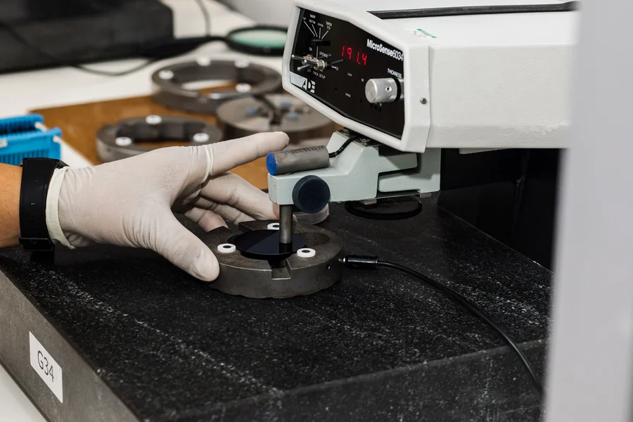
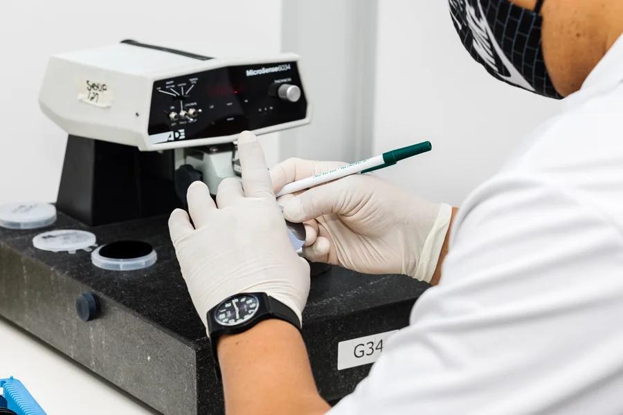
Accurate measurement allows manufacturers to determine whether thinning is producing the intended geometry. NIST has developed infrared interferometry methods to measure silicon wafer thickness and map thickness variations across wafer surfaces.
Metrology becomes particularly valuable when process adjustments are needed. Instead of relying solely on a final thickness value, manufacturers can evaluate variation across the substrate and use those measurements to understand better the outcomes of grinding and finishing operations.
For advanced three-dimensional integration, NIST also identifies wafer thinning, thin-wafer handling, processing, and bonding as manufacturing steps that present specific metrology challenges. This reinforces the importance of treating measurement as part of production control rather than simply an end-of-line check.
Choosing thin silicon wafers involves balancing target thickness with uniformity, surface condition, handling requirements, and subsequent processing needs. Wafer World can help you review available specifications and discuss substrate options based on your application. Contact us to schedule a consultation or call to discuss the dimensions and wafer characteristics your next project requires.




