Silicon is considered to be the integral building block of modern semiconductors, integrated circuits, rectifiers, diodes, solar cells, and transistors. Without it, you and I wouldn’t be able to enjoy TVs, cellphones, laptops, and other electronic devices. Even technology in the medical field and power devices make use of a silicon wafer. But how did silicon wafer come to be? Read on to know the brief history of silicon wafers.
Silicon was first discovered by a Swedish chemist named Jons Jacob Berzelius in 1824. This discovery didn’t immediately lead to any major industrial use, instead, Silicon was just seen as a chemical element. It was only in the 1940s when companies started to work on building some of the earliest transistors using a semiconducting material called Germanium. By the early 1950s, it was found out that Silicon was a much more efficient semiconducting material compared to Germanium. It was able to raise the power yield while reducing the operating temperatures. It was in 1954 when the first-ever commercial silicon transistor was produced, which paved the way for Silicon to be born in the transistor industry
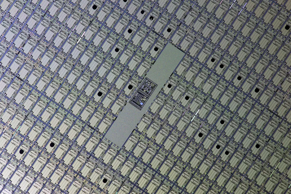
Today, Silicon is widely used in most integrated circuits, solar cells, transistors, and more in the form of wafer slices that are diced from a silicon ingot. The industry standard size for Silicon wafer is 300 mm in diameter. But wafer manufacturing companies have been working on increasing the size of wafers into 450 mm.

If not for the discovery of Silicon and the development of wafers, the world wouldn’t be able to enjoy the perks of modern technology. At Wafer World, you can get high-quality wafers in the best price possible. So, if you’re looking for a silicon wafer for your next project, you can contact us for any inquiries or get a quotation online!


