.webp)
Stay up-to-date with the latest news and trends in wafer and semiconductor technologies.
*Blogs are for educational and informational purposes ONLY
.webp)
To manufacture a GaAs wafer, gallium and arsenide first must be procured. Here, we’ll explore how GaAs is crafted—and if the USA can make it domestically in the future.
Read More
An InP wafer can find several uses, but it’s currently used in large quantities in quantum computing. Here, we’ll break down why.
Read More
Assessing the electrical properties of a material is crucial during silicon wafer manufacturing. Here are some of the key factors to look at.
Read More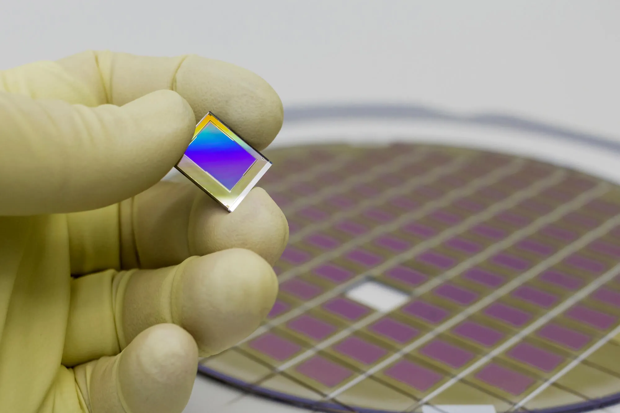
An FZ wafer is a safe material in its final solid form, but incorrect handling can be toxic and cause serious health problems, and here, we’ll explain why.
Read More
Lately, oversupply and decreased demand have made silicon prices drop—however, new tariffs could reverse this trend in the future, and here’s why.
Read More
Advances in bendy silicon can potentially change the game for silicon wafer suppliers. Let's explore the future of this phenomenon.
Read More
Did you know silicon wafer manufacturers dope silicon to enhance its electrical properties and improve it for certain applications? Learn more about some of these applications.
Read More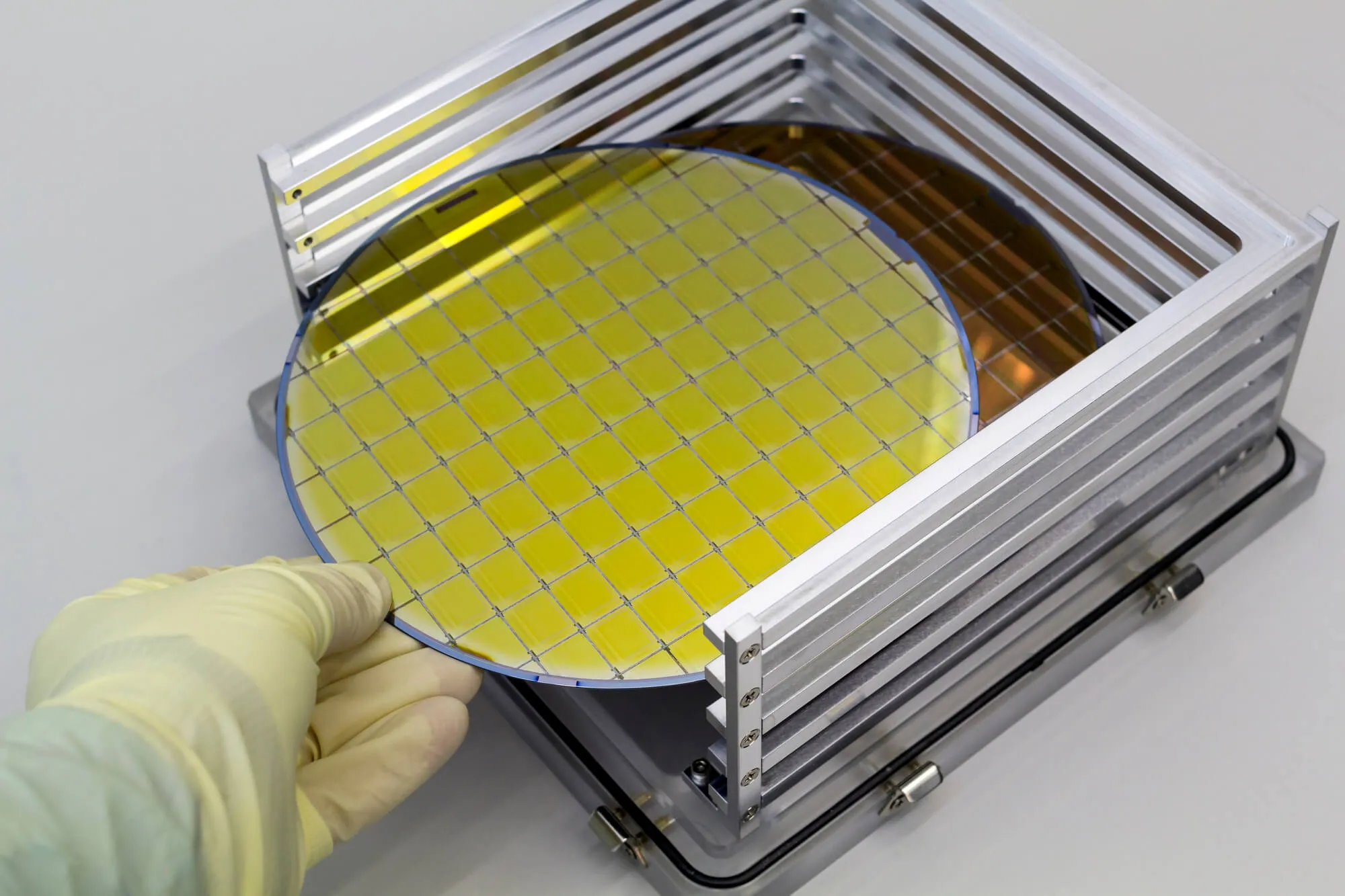
Band gap plays a crucial role in silicon manufacturing. Here, we’ll go more in detail about what band gap is and how it affects semiconductors.
Read More
Silicon wafer processing is an industry that’s always innovating. Here, we’ll explore some potential ways in which wafer manufacturing may evolve in 2025.
Read More
GaAs wafer’s superior efficiency in power management makes it an excellent component for wireless devices that depend on batteries. Let’s explain why.
Read More