.webp)
Gallium Arsenide is a fundamental material for semiconductors found in smartphones, satellites, and solar cells. Because it performs better than silicon in many high-frequency and high-power applications, GaAs wafers are often the go-to for high-speed electronic devices, becoming an irreplaceable material to our society.
However, rising geopolitical tension, tariffs, and new export rules have questioned the future supply of gallium to the United States. Here, we'll review the manufacturing process of Gallium Arsenide and assess the future of local GaAs wafer production.
Gallium arsenide (GaAs) is a compound semiconductor that has transformed the electronics and telecommunications industries. It performs better than conventional silicon in various applications due to the material‘s natural properties, such as a direct bandgap, high electron mobility, and thermal stability.
Gallium, a crucial component of this combination, is not uncommon in the Earth's crust. However, industrial, economic, and geopolitical factors make its extraction and acquisition costly.
This presents a problem for technology firms and wafer manufacturers that depend on GaAs because the US has not produced a single gram of gallium or arsenic since 1987.
.webp)
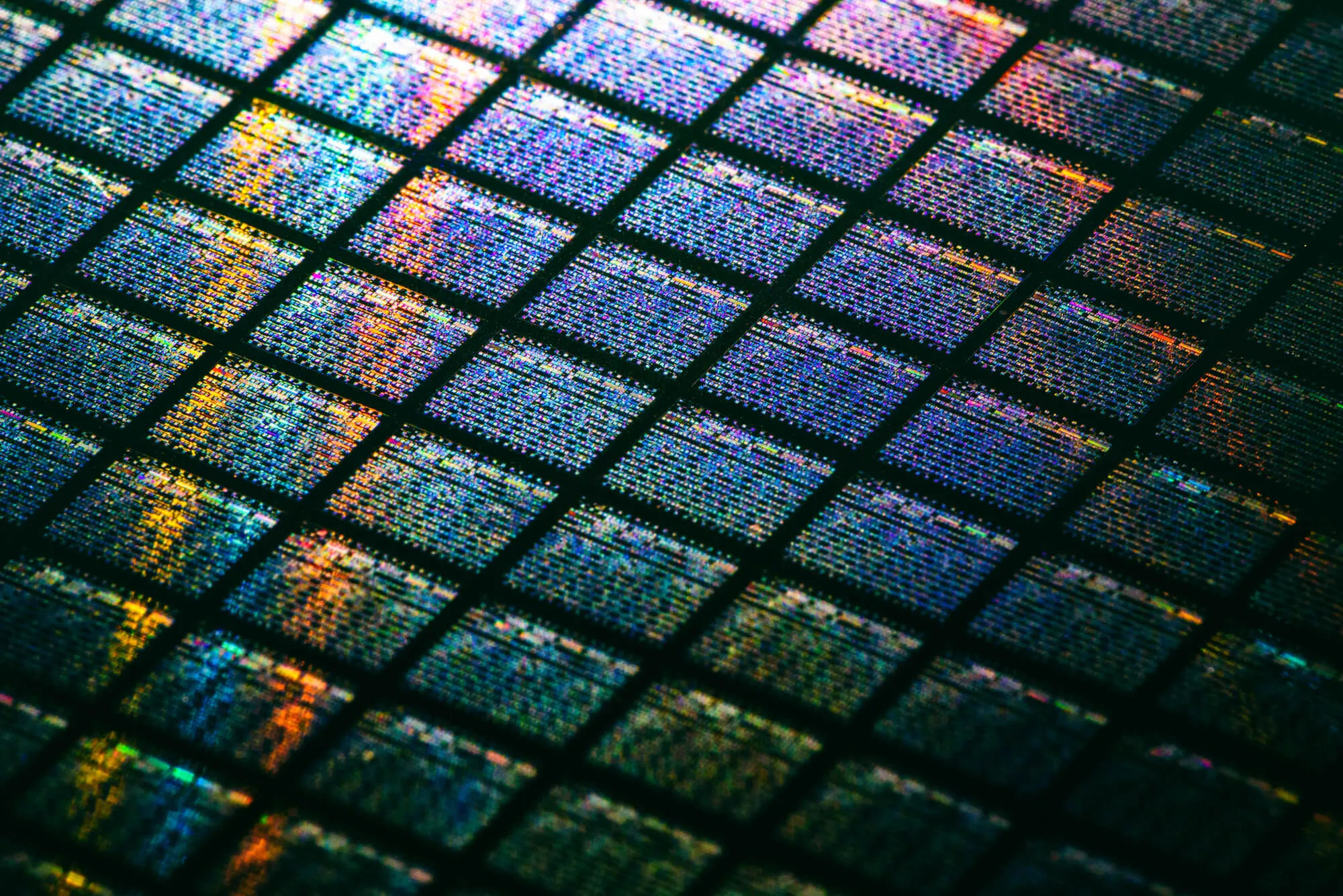
The base material gallium arsenide (GaAs) used in wafers is produced through a high-purity crystal growth process at controlled high temperatures. Specialized techniques can yield a high-quality base material suitable for advanced electronics and optoelectronics.
Let's explore this process in detail.
The first step in producing GaAs is obtaining raw materials. Gallium (Ga) is a byproduct derived from aluminum production residues (bauxite ore) and zinc ores. Following extraction, it is purified into high-purity gallium metal.
Arsenic (As) is typically obtained as a byproduct during the smelting of copper, lead, and gold ores. It is commonly processed into arsenic trioxide, which is then purified for use in semiconductor manufacturing.
Once the base materials have been acquired, the purified gallium and arsenic must be combined under carefully controlled conditions to produce GaAs. The most common method for producing the GaAs compound is the direct synthesis reaction:
This procedure is usually carried out in a sealed quartz ampoule using inert gas or vacuum to avoid oxidation. Arsenic is supplied in its tetrameric (As₄) form. To speed up the reaction, the ampoule is heated to between 600 and 800°C. Because of its high vapor pressure, arsenic must be kept under controlled conditions to avoid loss or explosion.
Following synthesis, the raw GaAs must be purified. There are two commonly used methods for this step:
These processes improve purity to 6N (99.9999%) or higher, which is required for electronic-grade materials.
The purified GaAs compound is then used to grow a single crystal ingot, as follows:
This is the most common method for producing single-crystal GaAs. Gallium and arsenic are combined in a crucible. The crucible is heated, and a seed crystal is dipped in the melt. The crystal is then gradually drawn upward during rotation, forming a sizable single crystal of GaAs.
Because arsenic is highly volatile at high temperatures, it is kept from evaporating by encasing the melt in boric oxide, which forms a protective layer throughout the process.
This method cools the molten material from the bottom up, promoting the growth of a single crystal as it solidifies. It is becoming increasingly popular in contemporary manufacturing because it is less costly and results in fewer defects than the LEC method.
Eventually, these ingots are cut into wafers to create semiconductor devices.
Only now can the GaAs crystal be shaped into wafers. Ingots are then sliced, polished, and cleaned.
A diamond saw is used to cut the single-crystal GaAs ingot into thin wafers. Then, the surface is chemically polished to achieve a smooth surface and lapped or flattened. This is significant because even minute flaws can impact the functionality of electronic components.
Lastly, wafers are meticulously cleaned in chemical baths to remove contaminants, residues, or particles.
To make the GaAs useful in electronics, the wafer’s properties need to be tailored by adding tiny amounts of other elements. This is called doping. The process occurs during crystal growth or afterward using ion implantation techniques.
There are two main types of doping:
Following polishing and doping, the wafers are prepared for use in the creation of devices such as:
Each wafer may undergo additional processes, such as photolithography, etching, and metal deposition, to create the finished semiconductor devices.
In the future, the United States could produce gallium arsenide (GaAs) domestically. However, doing so on a large scale would necessitate supply chain reorganization, strategic planning, and investment.
When zinc and bauxite (aluminum) are refined, gallium is a byproduct. Both metals are produced in the United States, and gallium has been recovered domestically. However, low market prices and competition from China caused most gallium extraction facilities to close.
In addition, the United States can extract and purify arsenic domestically, mainly in the form of arsenic trioxide, which is a byproduct of the smelting of copper, gold, and lead. However, handling and processing arsenic is sensitive due to environmental regulations.

Producing GaAs wafers is a complex, precise process that involves several steps. For that reason, the United States mostly imports its GaAs, already combined so that wafer manufacturers only have to slice and dope the crystals to make semiconductors. This will end up in high-performance electronics.
However, as worldwide tensions increase, we can’t help but wonder if the United States will be forced to resume its local GaAs production. Here at Wafer World, we're attentive to what is to come. Contact us today to learn more about our products and materials!


