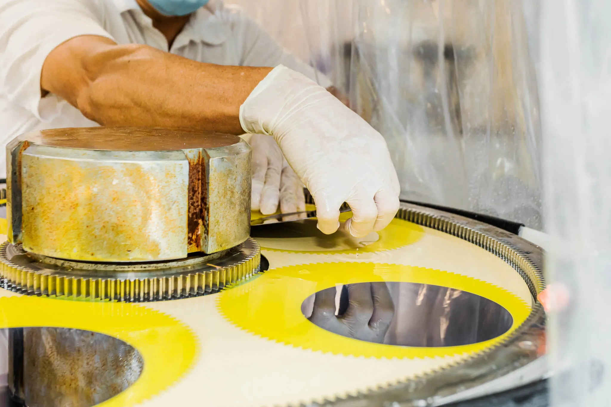
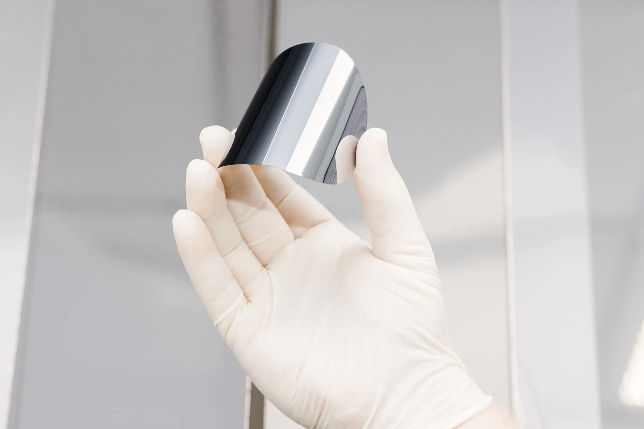
Gallium arsenide (GaAs) can be found practically anywhere, from cellphones to microwaves and LED lights. This material used in our GaAs wafer was a ground-breaking discovery for electronics, but it took time before humans were able to exploit it to its maximum capacity.
Nowadays, as technology advances, new materials are discovered, and geopolitics impact the trade of rare materials, the future of GaAs remains a mystery. Let’s go over a brief overview of what could wait for this semiconductor component.
Gallium arsenide (GaAs) is a gap semiconductor compound with a zinc blend crystal structure. Its acronym stands for Ga (Gallium) and As (Arsenide).
Gallium has a beautiful silvery blue appearance, and forms a brilliant mirror when painted onto glass. It’s not a very abundant mineral, with the same concentrations on the earth’s crust as nitrogen, lithium, and lead.
On the other hand, arsenic is usually found in sedimentary or igneous rock joined to or mixed with other elements, such as oxygen. If a metal compound is combined with arsenic, it’s called arsenide. The coordination of the metal is almost always octahedral or tetrahedral.
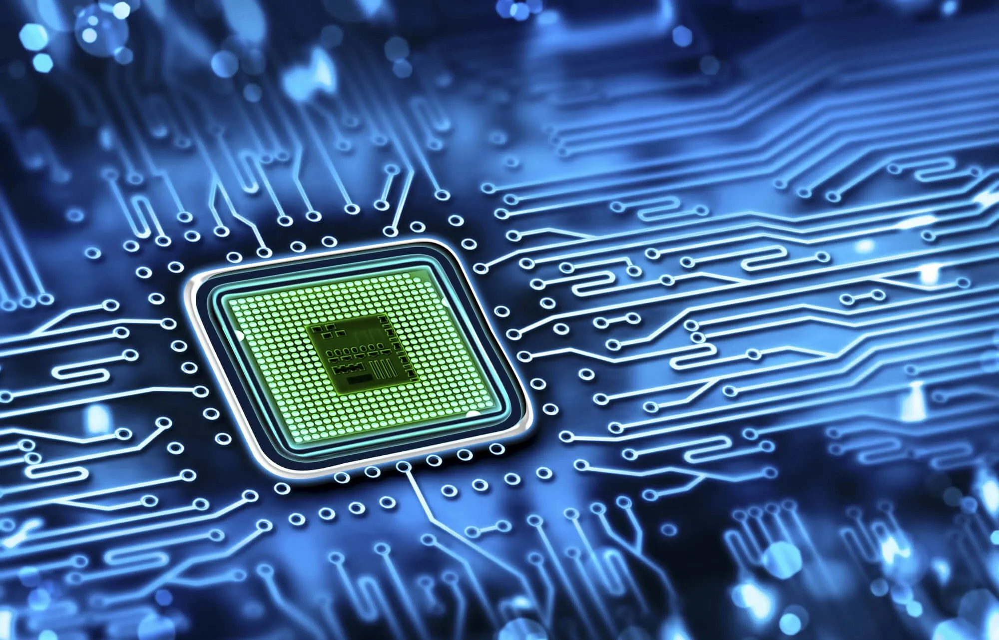
This material is used in the manufacture of devices such as diodes, integrated circuits (ICs), field-effect transistors (FETs), solar cells, lasers, optical windows, and even LED lights.
Its charge carriers, which are mostly electrons, move at high speed among the atoms. This allows GaAs semiconductors to operate at higher speeds and with lower power consumption compared to other semiconductor materials like silicon.
Additionally, GaAs devices can transmit data at high frequencies and generate less noise than other semiconductor components. So, they're great for weak-signal amplification and in the field of wireless communication.
The first record of Gallium was made in the late 18th century. This discovery is attributed to a French scientist named Lecoq de Boisbaudran, who was studying the element Zinc.
Arsenide, on the other hand, is a compound derived from arsenic, which was discovered by an alchemist known as Albertus Magnus or Albert the Great in 1250 AD. It was used in making rat poison and other pesticides.
Nevertheless, the history of gallium arsenide is complicated. For years, the technology required to produce GaAs devices wasn’t advanced enough to sort out the difficulty of the material itself and its processing and fabrication. Because of that, GaAs was labeled: “the semiconductor of the future, and it will always be that way.”
However, advances in compact disc technology, fiber-optic communications, and mobile telephony boosted investment in GaAs research and development. As a result, GaAs devices now enjoy stable niche markets.
As you can see, gallium arsenide is a material whose history dates from centuries ago. However, most of its uses have been found in recent years.
Here’s the historical background of gallium arsenide and its uses:
Gallium is one of the compounds of gallium arsenide used in electronics. Gallium can be found at low concentrations in sulfide minerals, in zinc ores, or associated with aluminum in bauxite. In fact, the main source of gallium is a by-product of aluminum refining.
According to the CRMA, around 80% is produced in China. The rest of the world’s production comes partly from Japan, Russia, and South Korea, according to USGS. Then, a smaller amount can be attributed to recycled material.
Only a few companies can make this element to the required purity for GaAs Wafers. One is located in Europe, while the rest are in Japan and China. Nevertheless, the Canadian company Neo Performance Materials also stated that they can develop gallium to the required purity.
Here are some statistics on the world’s gallium market from Reuters:
When it comes to arsenic, the largest producer in the world is also China, followed by Chile and Peru. USA hasn't produced arsenic since the 1985.
GaAs is still widely used in electronics applications today, but newer materials like silicon germanium and indium phosphide have emerged. Although these new materials perform better than GaAs, manufacturers still favor GaAs because it is a well-established technology.
In fact, Mordor intelligence estimates that the gallium arsenide GaAs wafer market will be of 1.18 Billion dollars in 2024. And this number will grow to 2.03 Billion in 2029.
After years of uncertainty, gallium arsenic finally fulfilled its promise of becoming the semiconductor of the future—which is our present.
Here at Wafer World, we believe that it’s important to know and understand the history of the materials we use to plan for the future. Gallium Arsenic wafers have a long way to go, but everything that has been achieved is thanks to the discoveries made by the people before us.
If you want to test the properties of this great semiconductor, gives us a call!


