.webp)
Silicon offers a tremendous commercial edge over other semiconductor materials since it costs around a thousand times less. Because of this, devices made of gallium arsenide (GaAs) and GaAs reclaim wafers are only employed in specialized applications where their unique advantages outweigh their higher price. Here's how this material can be produced at a lower cost.
.webp)
Researchers from Stanford University have now developed a manufacturing procedure that might significantly lower the cost of producing GaAs electrical devices and hence enable new applications for them, including solar panels. According to research, gallium arsenide-based solar cells are the most efficient at converting sunlight into power.
Gallium arsenide solar cells are limited to high-tech uses like satellites since silicon-based solar is much less expensive to manufacture. Since placing the satellite into orbit is the main expense, GaAs solar panels pay their freight thanks to their higher photon-to-electricity conversion efficiency.
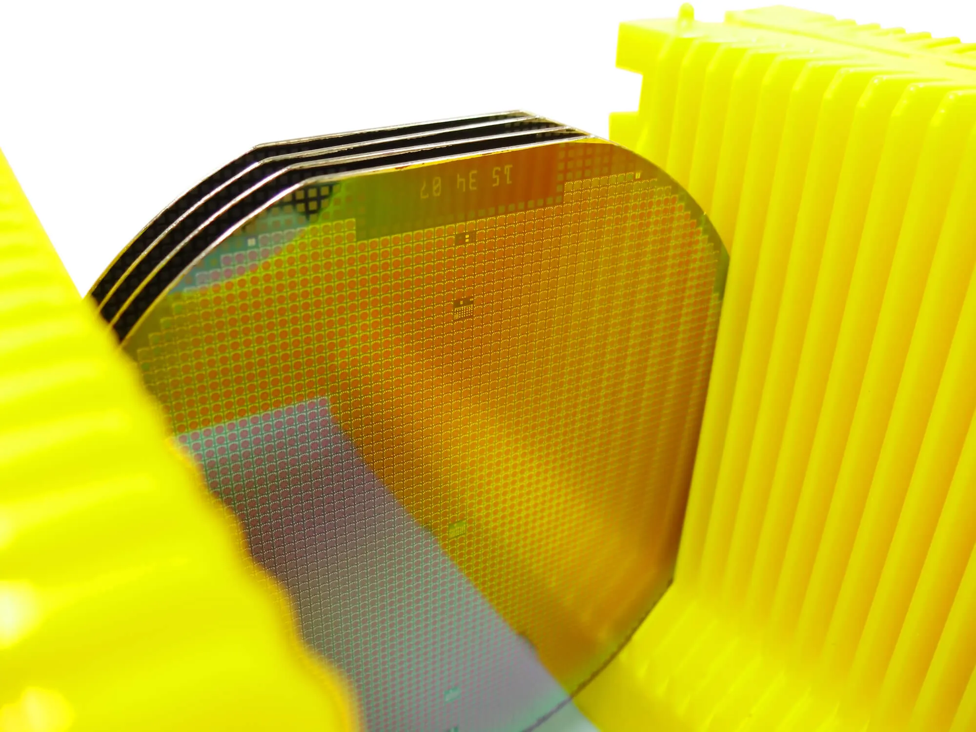
GaAs and silicon start on the same path from unprocessed crystal to the electronic device. Wafers, as they are known in the electronics industry, are created from both materials. These are material-purified flat, spherical platters. On top of these wafers, subsequent manufacturing processes produce computer chips, solar cells, or other electrical devices. However, it can cost up to $5,000 to produce a wafer of GaAs 8 inches in diameter instead of $5 for a silicon wafer.
By reusing the $5,000 wafer, the new Stanford approach aims to reduce this thousand-to-one cost disparity. Today, a GaAs device's functional electronic circuits are produced on top of this wafer. Gaseous gallium arsenide and other materials are flowed across the wafer surface to create this circuitry layer in the manufacturing process.
The Stanford approach would include numerous additional processes to make the wafer reusable. In their experiments, the researchers showed the technique. They initially placed a layer of throwaway material over the priceless wafer. On top of the disposable layer, they created a GaAs circuit layer using conventional gas deposition techniques. A laser destroyed the disposable layer, and the circuitry layer was lifted off like a pancake on a greased griddle.
At Wafer World, our team can provide high-quality materials for your business. Contact our team to learn more about the products we offer!


