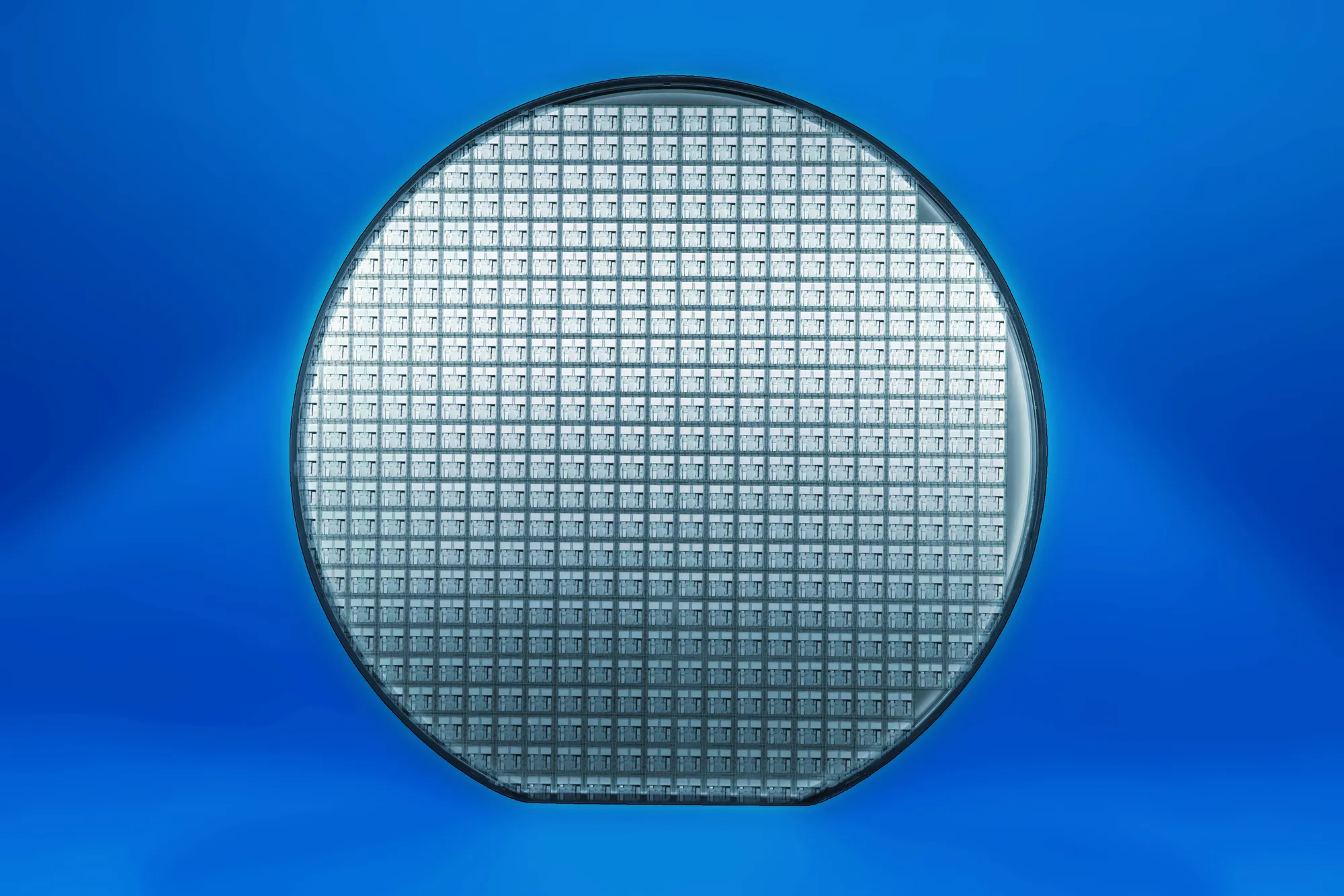
InP stands for Indium Phosphide. It is a binary semiconductor which belongs to the III-V semiconductors. An InP wafer is commonly used for high-frequency and high-power electronics and has an exceptional electron velocity compared to GaAs and Si. If you’re wondering what an InP wafer can be used for, then here are the different InP wafer applications:
LEDs and lasers based from InP are capable of emitting light at a very broad range. This can be used for fiber-based Telecom and Datacom applications. InP lasers are also eyed safe- the radiation cannot harm the retina. Optoelectronic terahertz is also utilized for ultra-sensitive spectroscopic analyzers, multilayer coatings detector for the automotive industry, and the measurement of polymers.
InP is commonly employed for telecommunications applications. An InP can produce highly efficient lasers, modulators, and sensitive photodetectors. It can also generate laser signals and convert and identify those signals back to its electronic form. Examples of the applications for telecom or datacom are the following:
Optical Sensing or spectroscopic sensing is all about the detection of harmful substances and environmental protection. Examples are:
High-speed microelectronics that utilize an InP wafer are considered to be one of the fastest devices accessible today. InP based microelectronics have High Electron Mobility Transistors or Heterostructure Bipolar Transistors. They are put together to form a circuit or modules for the following:

An InP wafer has superior properties which makes it more desirable for certain applications. If you’re looking for a high-quality InP wafer, then at Wafer World you can get high-quality InP wafers at the best price possible. Call us for inquiries or purchase wafers online!


