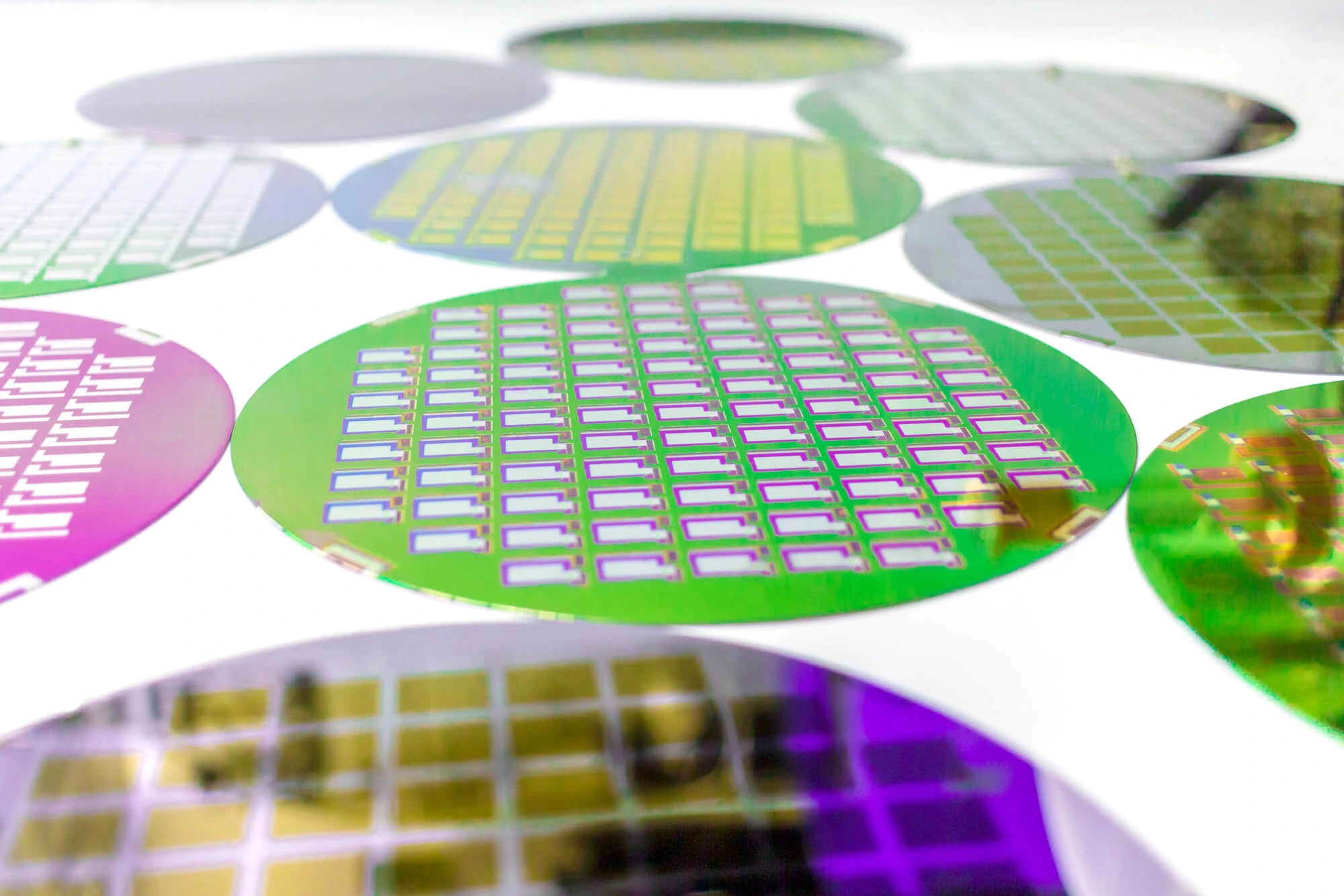
In silicon wafer manufacturing, size matters—more than ever. As semiconductor technologies advance, selecting the right wafer diameter is not just about staying current but also about optimizing for cost, yield, tool compatibility, and process efficiency.
The most common wafer sizes in use today are 200 mm (8 inches) and 300 mm (12 inches), while 450 mm (18 inches) wafers remain largely in the research and development (R&D) and pilot phases. Each has distinct advantages—and choosing the wrong size for your process can mean higher costs, lower yields, or wasted fab capacity.
Silicon wafer diameters have steadily increased over the decades to enable more chips per wafer, better manufacturing economics, and higher throughput.
200 mm wafers became the industry standard in the 1990s. In the early 2000s, 300 mm wafers became the standard because they enabled high-volume, advanced-node production. On the other hand, 450 mm wafers have been in development for years but have yet to see mass adoption due to extreme costs and infrastructure challenges.
Larger wafers offer a greater surface area, allowing more chips to be placed per wafer, which in turn results in a lower cost per die if yields are well-managed. But with each increase in size comes new capital investment, cleanroom upgrades, and greater process control complexity.
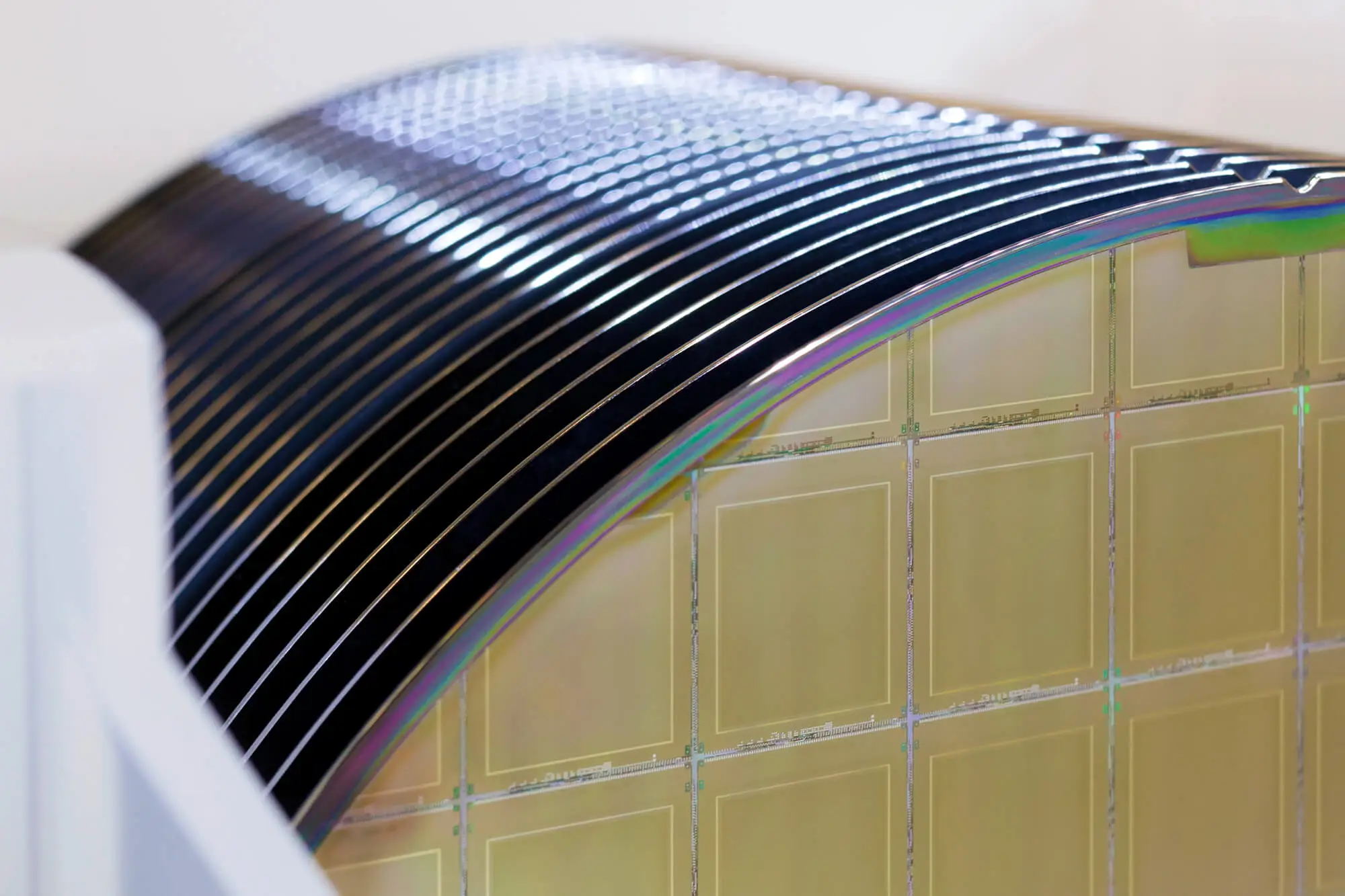
The most direct benefit of larger wafers is the increase in usable silicon surface area. Here's how they compare:
This surface area directly translates to die count per wafer, which significantly influences cost amortization. Assuming similar defect density and chip sizes, 300 mm wafers yield more than twice as many dies as 200 mm wafers. 450 mm wafers, in theory, could cut cost per die even further—but only with advanced process control and minimal edge losses.
Die yield per wafer isn’t just about size—it’s about defect density and edge exclusion. Larger wafers experience proportionally less edge loss, meaning they use silicon more efficiently. However, they also require tighter process control, as a defect on a 300 mm or 450 mm wafer affects more die than on a 200 mm wafer.
Larger wafers significantly reduce cost per die—but only when high yields and full utilization are achieved. The trade-off is higher upfront capital costs, including:
For example, shifting from 200 mm to 300 mm requires major retooling, often costing billions for high-volume fabs. However, for high-throughput applications like CPUs, GPUs, and mobile SoCs, the ROI is strong due to the lower per-chip cost.
In contrast, 200 mm remains economically viable for lower-volume or specialty applications, where equipment reuse and process maturity outweigh the benefits of wafer size scaling.
Wafer size also determines which process nodes and tools are available. Not all wafer sizes support all levels of technology:
As mentioned, each wafer size aligns better with different types of device production:
Mixed strategies are also common: many IDMs and foundries run multi-wafer-size operations, balancing R&D, prototyping, and high-volume manufacturing across both 200 mm and 300 mm lines.
While 450 mm wafers offer the potential for dramatic cost savings and throughput gains, they remain mostly theoretical. Development stalled due to the immense capital investment required and a lack of standardized equipment.
450 mm wafers still offer low ROI, as chiplet-based design, heterogeneous integration, and advanced packaging can still be done on existing wafer sizes. As a result, many believe the future lies not in wafer scaling, but in design-level optimization and packaging innovations that work within current 300 mm ecosystems.
If you’re working on low- to mid-volume production, especially for analog, MEMS, or power devices, 200 mm remains cost-efficient and reliable. Toolsets are mature, and the ecosystem is stable.
If you’re producing high-density ICs at advanced nodes—think CPUs, GPUs, AI accelerators, DRAM, or NAND—300 mm is essential. Despite higher fab costs, the yield and throughput gains pay off at scale.
If you’re planning for the future, 450 mm isn’t yet a realistic option—unless you're a Tier 1 foundry or research institution exploring next-gen manufacturing models.
Choosing the right wafer size is a strategic decision that balances cost, process capability, yield, and application fit. While 450 mm may be the horizon, today’s semiconductor landscape is still driven by 200 mm for legacy and specialty nodes and 300 mm for advanced, high-volume logic.
Understanding how these wafer sizes impact your tools, processes, and business goals is essential to staying competitive in silicon wafer manufacturing. And if you need help, Wafer World is here for you. Reach out today, and let’s work together to find the right wafer size for your project!


