Silicon wafer processing is at the heart of modern electronics manufacturing. It is the fundamental technology that enables the production of integrated circuits, microchips, and other semiconductor devices that power our digital world. In this blog post, we will provide an introductory overview of silicon wafer processing, exploring its importance, key steps, and its role in shaping our technological landscape.
.webp)
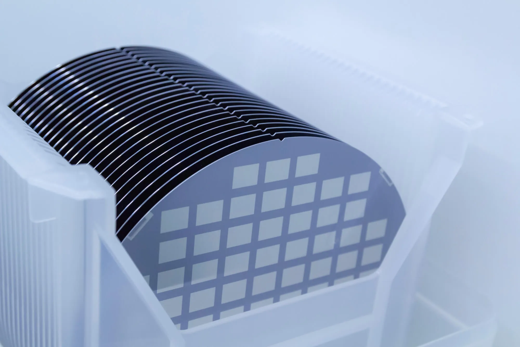
Silicon wafers serve as the substrate upon which semiconductor devices are fabricated. Silicon is chosen for its unique electrical properties, high purity, and abundant availability. The processing of these wafers involves a series of intricate steps, each crucial to the performance and functionality of the final product.
The process begins with the production of a high-purity silicon crystal. This crystal is then sliced into thin wafers using precision cutting techniques. The wafer's orientation and crystal structure significantly impact its electronic properties.
Wafers undergo rigorous cleaning and polishing to remove impurities and defects on the surface. This step ensures a pristine foundation for subsequent processes.
The Controlled introduction of specific impurities (dopants) is used to modify the electrical properties of the silicon. This step is crucial in creating p-n junctions and enabling transistor operation.
Thin layers of materials like silicon dioxide or metal are deposited onto the wafer using techniques such as chemical vapor deposition (CVD) or physical vapor deposition (PVD).
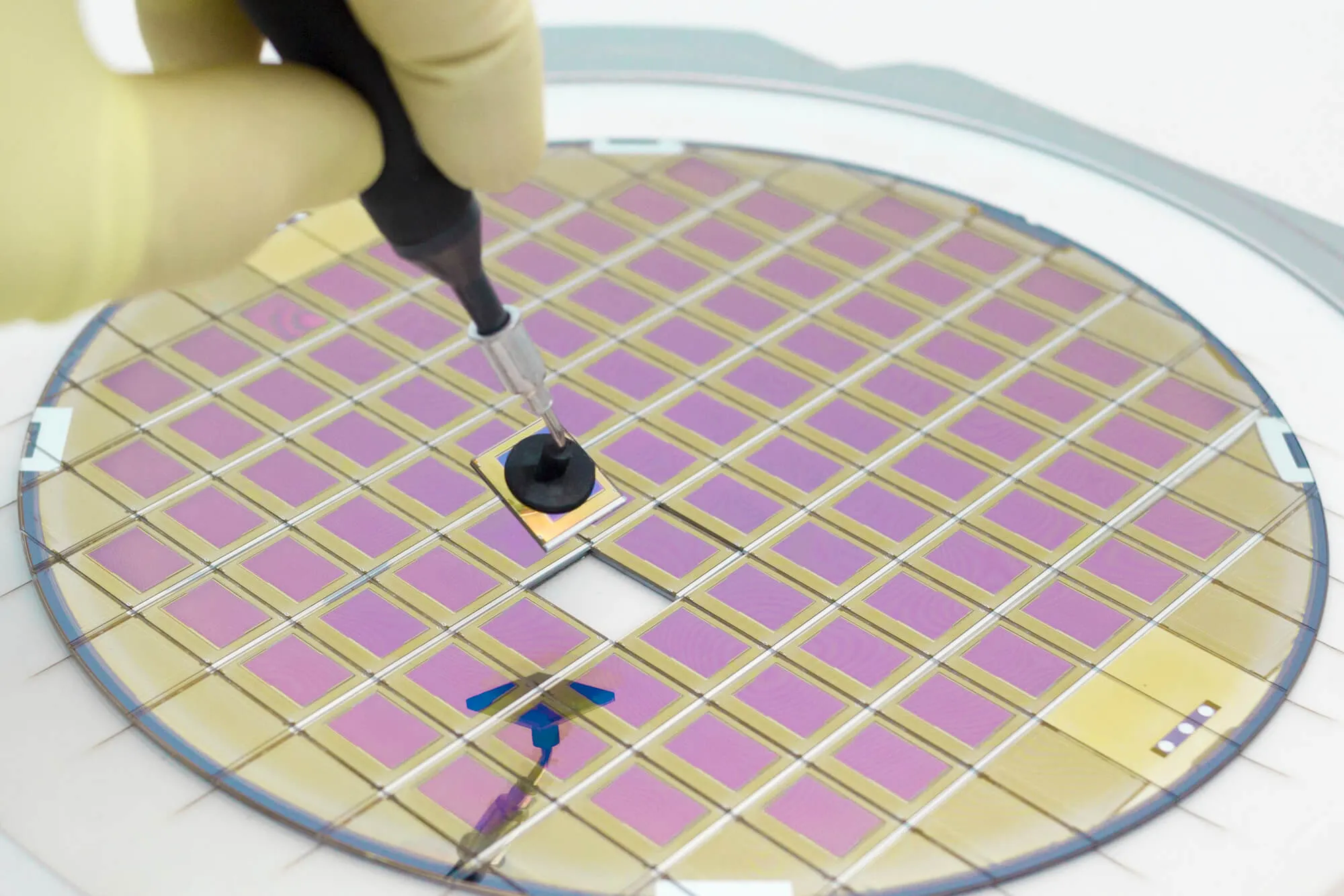
Photolithography is a key step in defining the intricate patterns of the semiconductor device. It involves projecting a mask pattern onto the wafer and selectively exposing it to light.
Unwanted materials are removed from the wafer's surface through chemical or plasma etching, leaving behind the desired pattern.
Further doping is often needed to fine-tune the electrical characteristics of the device.
Heat treatment processes are used to activate dopants and repair damage caused by previous steps.
Finally, each chip is tested for functionality, and the wafers are cut into individual chips, which are then packaged for use in various electronic applications.
Silicon wafer processing is a highly specialized field, and continuous advancements in technology have enabled the creation of smaller, faster, and more energy-efficient electronic components. From smartphones to supercomputers, silicon wafers are the foundation of the digital age, making them a vital component of our modern world. Wafer World has the capacity to provide you with high-quality wafers for your business needs! Call us today!


