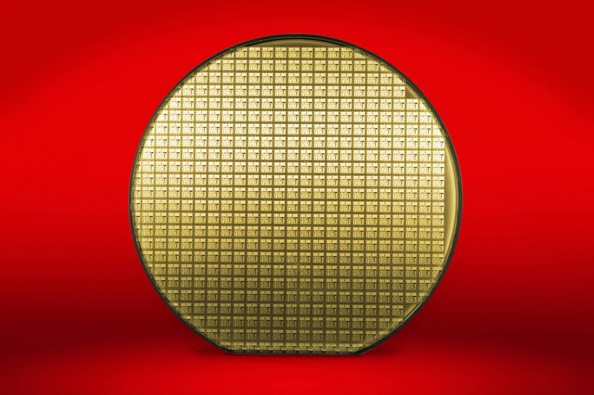
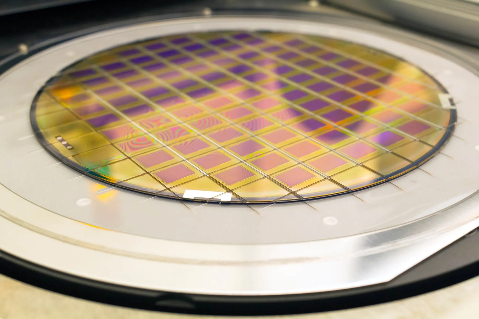
Silicon wafers are the backbone of modern electronics, the foundation for integrated circuits and semiconductor devices. Among the various methods used for silicon wafer production, the Float Zone (FZ) method and the Czochralski (CZ) method are two prominent techniques.
In this comprehensive comparative analysis, we will delve into the strengths and weaknesses of FZ wafers and CZ wafers, shedding light on the critical factors that distinguish these technologies.
FZ wafers are synonymous with high purity and low defect density, making them an excellent choice for applications demanding stringent quality standards. The float zone method involves melting a polycrystalline silicon rod at its tip and slowly pulling a single crystal from the melt. This process eliminates impurities and crystal defects, producing a nearly perfect silicon crystal structure.
Czochralski (CZ) wafers, a more common and widely adopted technology, are produced using the Czochralski process. In this method, a seed crystal is dipped into a molten silicon melt, and a single crystal ingot is slowly pulled from the melt. While CZ wafers may not achieve the same purity levels as FZ wafers, they remain the industry workhorse for many applications.
When selecting between FZ and CZ wafer technologies, carefully weighing their relative strengths and limitations is key to choosing the optimal solution. Both offer distinct advantages that make them suitable for different applications and production scenarios. Conducting a comparative analysis enables a nuanced understanding of how these technologies align with specific priorities around performance, cost, scalability, and defect tolerance.
A careful comparative analysis should examine metrics like:
FZ wafers excel in terms of purity and low defect density, making them ideal for applications where high-quality silicon is paramount. On the other hand, CZ wafers may not achieve the same level of purity, but they are suitable for a wide range of applications where moderate purity is acceptable.
FZ wafers may have a cost disadvantage due to the intricacies of the float zone process, coupled with lower throughput. With their higher throughput and established manufacturing processes, CZ wafers are more cost-effective for large-scale production.
FZ wafers find their niche in applications requiring the utmost purity and minimal crystal defects, such as advanced semiconductor manufacturing, high-performance electronics, and precision optics. CZ wafers, being more cost-effective and versatile, are preferred for mainstream semiconductor applications, photovoltaics, and a range of electronic devices.
The landscape of silicon wafer technology is not static; it's a dynamic realm where innovations and advancements continually redefine the possibilities. As we navigate the future, several emerging trends are influencing the trajectory of both FZ and CZ wafers.
Researchers and manufacturers are exploring hybrid approaches that combine the strengths of FZ and CZ technologies. These endeavors aim to harness the purity of FZ wafers while benefiting from the cost-effectiveness and scalability of CZ production. This hybridization could potentially bridge the gap between ultra-high purity and large-scale production demands.
The CZ technology is not resting on its laurels. Ongoing research focuses on refining the Czochralski process to further reduce crystal defects and enhance the purity of CZ wafers. As CZ wafers become cleaner and defects are minimized, they may encroach further into applications traditionally dominated by FZ wafers.

In the realm of silicon wafer production, the choice between FZ wafers and CZ wafers ultimately depends on the specific requirements of the application. FZ wafers set the standard for purity and low defect density but come at a higher cost, making them suitable for specialized applications. On the other hand, CZ wafers continue to dominate the semiconductor industry for mainstream applications with their cost-effectiveness and versatility.
As technology advances, both methods will likely undergo further refinement, pushing the boundaries of what is achievable in terms of wafer quality and cost-effectiveness. Call us for more info!


