GaAs reclaim wafers are widely used in semiconductor testing environments to reduce costs while maintaining realistic process conditions. However, testing with GaAs reclaim wafers requires a different mindset than testing with prime wafers or silicon substrates.
GaAs is mechanically fragile, thermally sensitive, and electrically distinct. If reclaim-specific considerations are ignored, test data can become unreliable—or worse, wafers can fail during probing, thermal cycling, or handling. Fortunately, by adhering to best practices for testing with GaAs reclaim wafers, you can maximize value while ensuring data integrity, protecting equipment, and maintaining downstream processes.
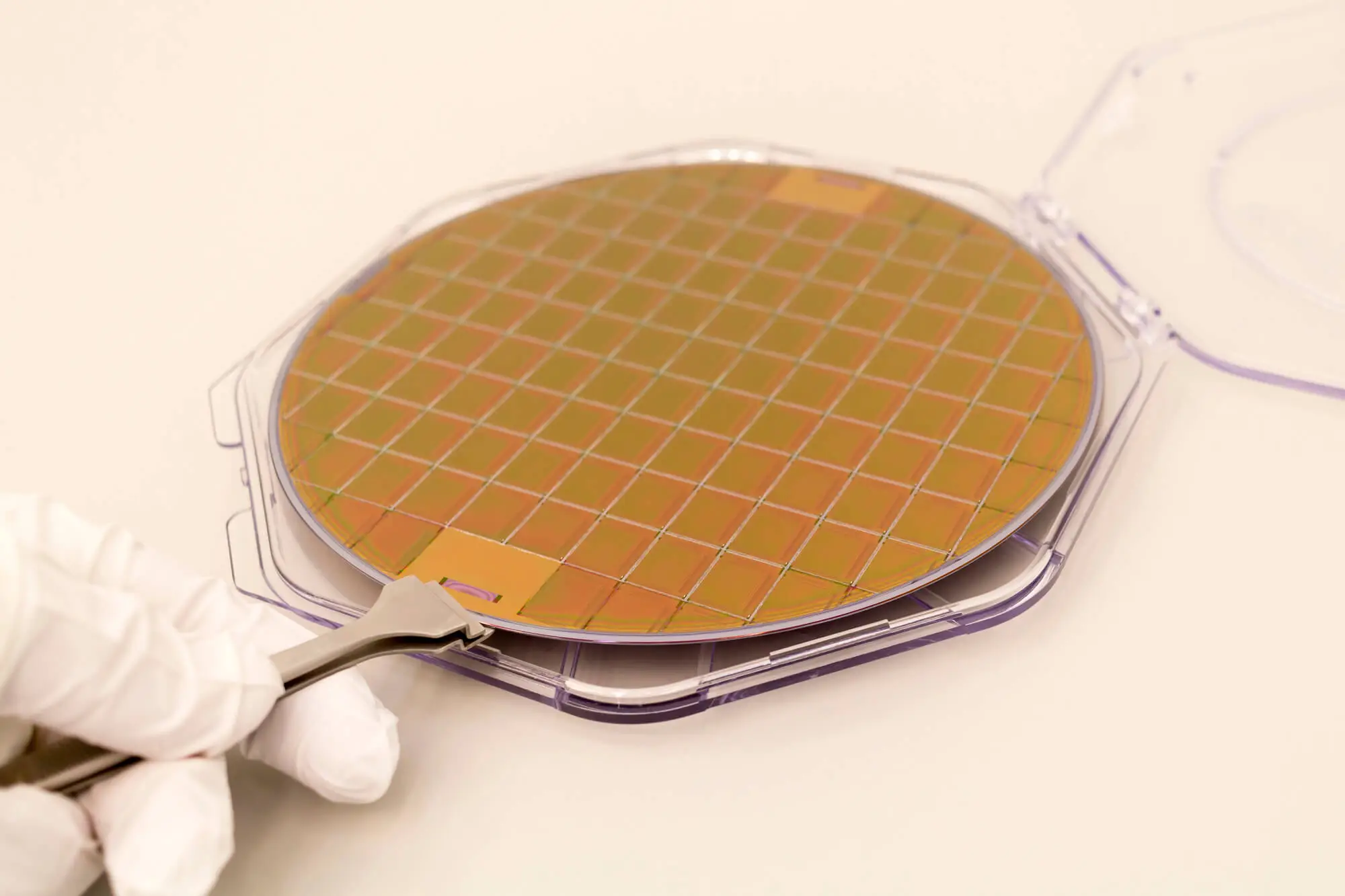
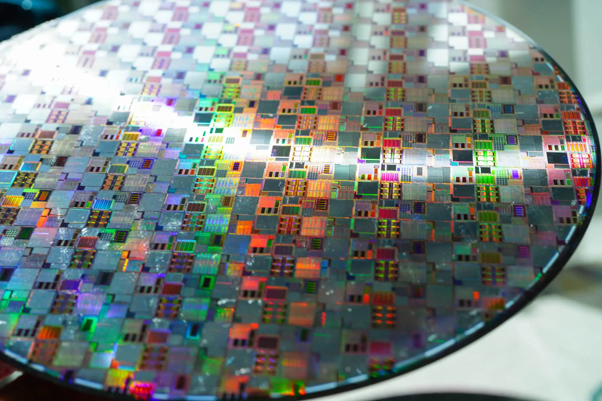
Gallium arsenide (GaAs) wafers are semiconductor wafers made of GaAs substrate material. They’re ideal for high-frequency and high-speed electronic devices, such as microwave and millimeter-wave applications, high-power and high-frequency transistors, and optoelectronic devices; however, they are also expensive.
For that reason, using GaAs reclaim wafers can be a valuable strategy for fabs. When sourced and prepared correctly, GaAs reclaim wafers provide the same material properties as prime GaAs wafers at a fraction of the cost—making them ideal for non-product testing. They are commonly used for:
However, reclaimed wafers should not be treated as “lower-risk” substrates. Their prior processing history and altered surface conditions require disciplined testing practices to ensure yield and performance outcome.
Before defining a test strategy, it is essential to understand how GaAs behaves differently from silicon, particularly in its reclaimed form.
Certain GaAs characteristics affect testing, such as:
Luckily, there are certain practices you can enforce to prevent these issues.
Not all GaAs reclaim wafers are suitable for testing. Before wafers enter a test flow, verify their:
Request their reclaim specifications and inspection data from your supplier, not just diameter and orientation. For electrical or RF testing, surface defects can distort results—even if devices are not being fabricated at the time.
GaAs reclaim wafers are ideal for process-representative testing, but they are not a universal substitute for prime wafers. Using GaAs reclaim wafers is recommended for:
However, it’s better to avoid using reclaimed wafers for:
To prevent data misuse, we also recommend that you clearly label reclaim wafers in MES and test documentation.
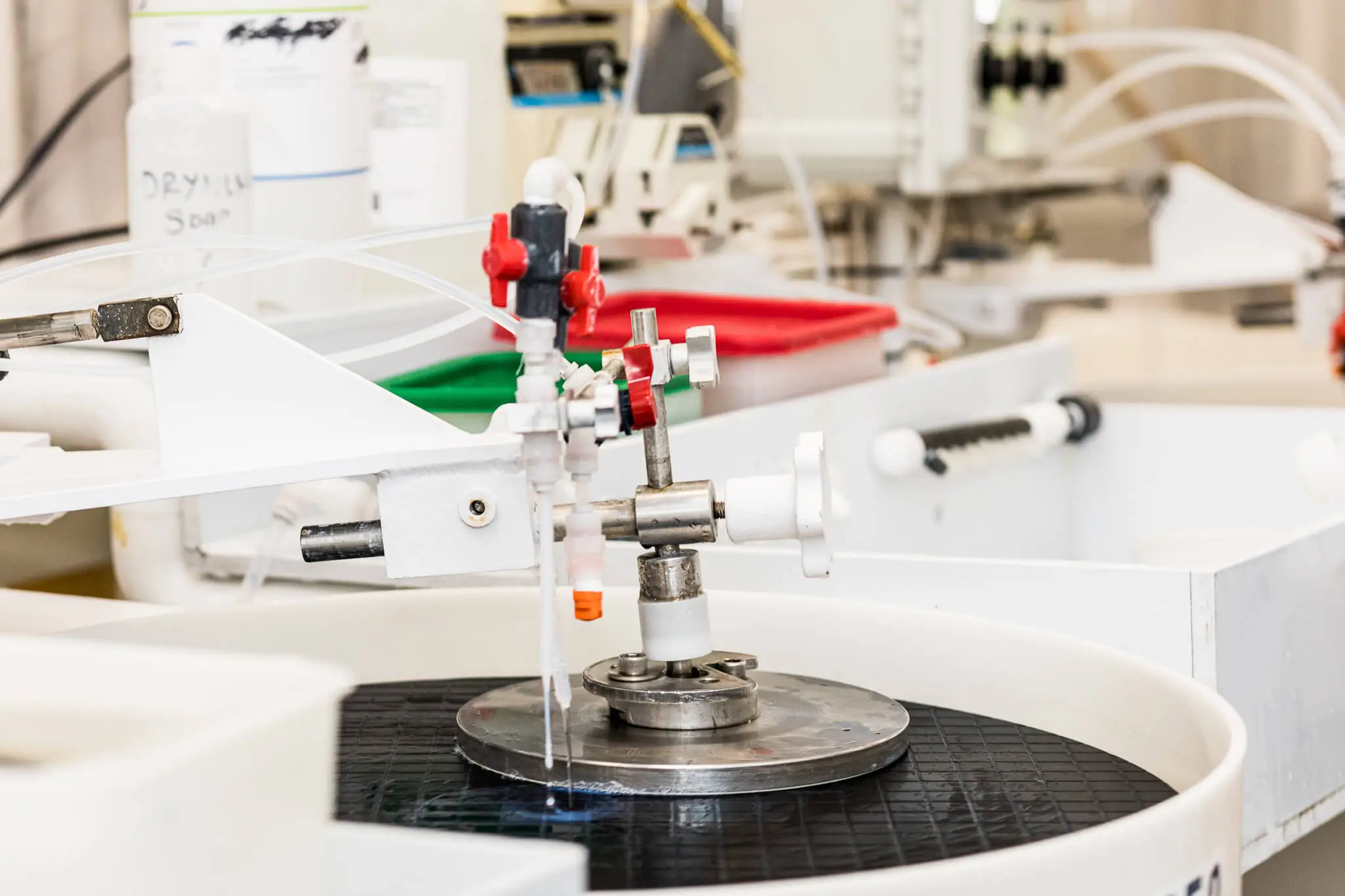
One of the most common failure modes when testing GaAs reclaim wafers is overaggressive probing. Key probing adjustments include:
GaAs is more prone to surface cracking and pad damage, especially on reclaimed surfaces where mechanical strength may be slightly reduced. Luckily, proper probe optimization extends wafer life and improves measurement repeatability.
GaAs has lower thermal conductivity than silicon, which means heat dissipates more slowly during testing. This can lead to many risks, such as:
To prevent that, use conservative current limits and allow adequate cool-down time between tests. Additionally, we recommend you validate chuck temperature accuracy and avoid prolonged high-power RF stress on reclaim wafers. Thermal damage may not be visible immediately—but it can compromise subsequent test runs.
GaAs reclaim wafers may have experienced prior high-temperature processes, chemical exposure, or CMP and repolishing. As a result, electrical baselines should never be assumed to be accurate. Before running experiments or collecting comparative data:
This ensures that test conclusions are based on current wafer condition—not historical assumptions.
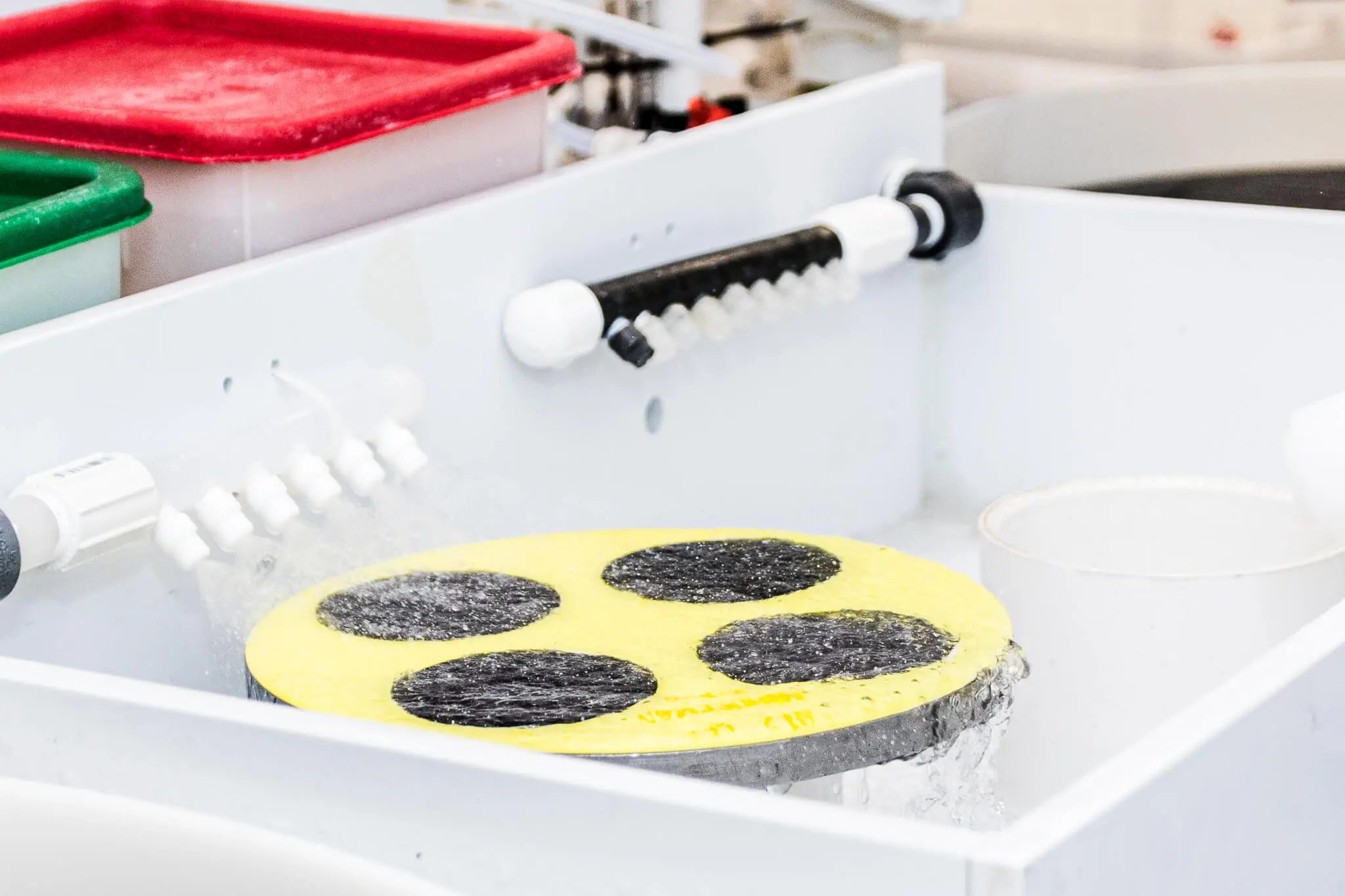
Mechanical damage is a leading cause of reclaiming wafer loss during testing. Handling best practices include:
Even small edge chips can propagate into catastrophic wafer breakage during probing or thermal cycling.
A major advantage of reclaim wafers is reusability—but only if usage is tracked. For that reason, we recommend you track:
Overusing reclaimed wafers without tracking can lead to inconsistent results and unexplained failures.
When used correctly, GaAs reclaim wafers deliver:
For fabs, IDMs, and test houses, this translates into higher throughput and lower development costs—without sacrificing realism.
Avoid these frequent issues:
Each of these mistakes can undermine confidence in test results and negate cost savings.
GaAs reclaim wafers are a powerful tool for testing, qualification, and development—but only when best practices are applied intentionally. By aligning probing, thermal control, handling, and data interpretation to GaAs reclaim realities, engineering teams can reduce costs without compromising test integrity.
Used correctly, GaAs reclaim wafers are not a compromise—they are a competitive advantage. Do you need extra tips for testing with GaAs reclaim wafers? Contact Wafer World for help!


