The world of wafer semiconductors is filled with materials that can do the job effectively. Although silicon is undoubtedly the most popular element of the bunch, many other options are well-suited for different applications. Just listing the acronyms alone might make your head spin; FZ, InP, Si, oh my!But one, in particular, is quickly becoming a top option and that is Gallium Arsenide or GaAs wafers. As leaders in the semiconductor industry, Wafer World aims to educate our readers about their options, and today we will highlight GaAs wafers – what they are, how we use them, and how we make them.


The answer to ‘what is a semiconductor?’ lies in the name. In essence, semiconductors are materials that can transfer electricity at a rate somewhere between a conductor and an insulator. The reason semiconductors are essential in manufacturing electronic equipment is that they make it easier to regulate the flow of electricity between different components.
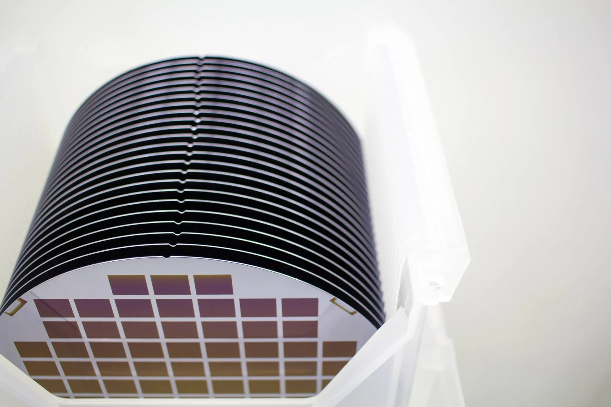
Wafers are the underlying layer of the conductive material used in micro-electric devices. Because they are so thin and as a result of the extensive manufacturing process that goes into creating them, they are especially suited to transfer currents in integrated circuits or photovoltaic cells used in solar panels.
‘GaAs’ is shorthand for Gallium Arsenide, a compound made up of two elements, and the semiconductor used to manufacture GaAs wafers. GaAs is used as a direct bandgap semiconductor, which in layman’s terms, simply means that particles such as electrons can pass through components much quicker and with very little interference. This makes them particularly useful in optical devices because photons, the basic unit for all light, can pass through lenses with ease.
The use of GaAs wafers is dictated by the capabilities of the compound. Because GaAs is a direct bandgap semiconductor, it is especially useful in sensitive electronic equipment that requires amplifying low frequencies. Some of the most common applications for GaAs wafers include:
Although not massively different, GaAs wafers do carry some properties that make them more effective than silicon wafers in certain applications. For example, GaAs wafers are much more resistant to radiation which makes them better suited for defense and aerospace applications. GaAs also transfer light more effectively than silicon which is why they are preferred in LED manufacturing.
Although GaAs wafers do have several attributes that make them superior to the silicon variety, silicon wafers still make for the more practical option. For starters, silicon is not a compound, which means that less chemistry is involved. Silicon is also extremely abundant and the manufacturing process for silicon wafers tends to be more cost-effective. However, recent advancements have made GaAs wafer manufacturing less expensive and the electronic equipment they are used with more abundant so this trend might soon be changing.
As we mentioned, GaAs is a chemical compound made up of two elements, Gallium (Ga) and Arsenic (As). To obtain the final product, the first step is combining these elements in a high-pressure, high-temperature vessel. When the materials reach over 800 degrees Celsius, they melt and combine. Once the chamber has had a chance to cool down, what remains is a Gallium Arsenide ingot that can then undergo further manufacturing.
There are multiple processes for creating the crystal from which the final wafer will be cut. The most popular method for larger applications is the Czochralski process which involves melting the compound in a crucible then spinning a ‘seed crystal’ which accumulates the substance before cooling. This process leaves behind a larger GaAs crystal which can then be fully processed before creating the wafers.
Once we obtain a fully realized GaAs crystals they are mounted in front of a specialized saw before they are sliced into wafers. The thickness of each GaAs wafer is dependent on its use and they can range anywhere from 50mm to 300 mm.
Polishing is one of the most important processes of GaAs wafer manufacturing. These thin components are responsible for transmitting microscopic particles that are highly sensitive and can be easily interfered with by even the slightest abnormalities. For this reason, thorough polishing ensures that the wafers achieve their optimal capacity as semiconductors.
This step is almost as important as polishing for the same reasons. During the manufacturing process, wafers can accumulate particulates on the surface that can interfere with signals and currents. Cleaning them requires specialized equipment and using a ‘clean-room’ to avoid any contaminant from landing on the surface of the GaAs wafer.
After the GaAs wafers have been formed, cut, polished, and clean, the last step is to make sure they stand up to the real-world conditions they will be exposed to. Testing involves simulating how the wafers will be used including exposing the materials to high temperatures and other stressors.
With all the manufacturing steps completing, the last thing to do is packing up the GaAs wafers. This is done in specialized cassettes and sealed to avoid any damage while they’re transported.The final product is highly sensitive and prone to scratching so we take great care to package the wafers as securely as possible.
For decades, Wafer World has cultivated a reputation as one of the leading semiconductor wafer manufacturers because of the exceptional quality of our products and our commitment to educating our clients. If you are in the market for high-quality wafers or simply wish to learn more, please browse our website or take a look through our inventory. Looking for a quote? Just click here!


