Buy silicon wafer because it offers various benefits no other semiconductor material can provide. It's the most common type of wafer used in most applications because of its abundance and superior quality. If your business or next project has something to do with wafers, here are the reasons why you should choose silicon wafers:

Silicon wafers are made from highly pure silicon, which is used to grow silicon ingots. It is then sliced into wafers through the method called wafering. Pure polycrystalline silicon wafers are used for photovoltaics applications, while extremely flat single-crystal silicon wafers are used for manufacturing computer chips and integrated circuits.
Silicon wafers can be grown through the FZ or float zone method. The FZ method is a process that allows wafers to be produced in a way that optimizes their properties. It also allows higher growth rates and decreases light impurities' concentration levels that help prevent the formation of defects and control resistivity throughout the entire wafer. Plus, the production cost is cheaper and faster.
Buy a silicon wafer because it has multiple applications. Its excellent mechanical properties and high heat resistivity are useful for MEMS applications and high-temperature applications. Its high performance and low power consumption make it suitable for telecommunication applications. It's also used to produce high-speed electronic devices, light-emitting devices, UV detectors, solar cells, computers, microprocessors, integrated circuits, and more.

Silicon wafers are highly effective for high-powered devices because of its wide bulk resistivity spectrum, reduced resistivity tolerances, radial resistivity deviation, high minority carrier lifespan, and more.
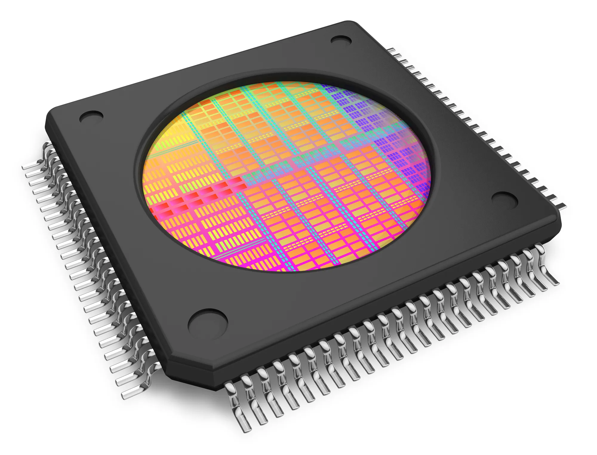
What is a Silicon Wafer?
A silicon wafer finds its use in semiconductors that form an essential part of all electronic devices. It is an ultra-flat disk and has a mirror-like surface. Polishing silicon wafers make them free from any irregularities. If wafers are going to function correctly, they need to be clean of any impurities.Otherwise, manufacturers cannot use them as substrate materials in the semiconductors. Apart from polishing, wafer manufacturing involves several other steps. A few of them are slicing, grinding, and rounding.
Silicon Wafer Processing
Silicon wafer processing involves various steps. The process begins with coating the silicon wafer with layers of thin glass and nitride.
Photolithography
The next step involves coating the wafer uniformly with photoresist when it is spinning. The photoresist is a light-sensitive liquid. Photoresist gets exposed via a simple process.The process begins with the earmarking of certain portions of the wafers. These portions are then exposed to ultraviolet light. However, between the light source and wafers, comes the mask. This mask allows light to pass through its transparent areas to expose the photoresist.Choose From A Wide Selection Of High-Quality Silicon Wafers, Ready To Ship. Get in touch with us to Buy Silicon wafer.
Direct Wafer Stepping
The images find their way onto the wafers through optics. In this method, the mask is no longer in proximity to the wafer. This method allows the use of a larger mask. It helps to achieve better resolution on the photoresist through manipulations.When exposed to ultraviolet light, the photoresist solidifies and becomes immune to etchants. This step makes it easy to keep only the solidified photoresist on the wafer.
Etching
Etching follows the photolithography process. This process makes the wafer free of any foreign materials. The two most popular methods used are wet etching and dry etching. Etching leaves a mask-like pattern on the wafer and is central to its function. Cleaning the solidified photoresist using another chemical is a part of this process.
Masking
It involves implanting dopants in unprotected areas. It changes the electrical features of earmarked areas of the integrated circuit. The dopants play a role in encouraging or discouraging the passing of current across the die.The repetition of these steps offers layers of glass, polysilicon, and aluminum. Dopants typically include phosphorous, boron, and arsenic. If the wafer suffers from any damages, annealing, a heating process, reduces them.
Wire Bond
This process includes creating an electrical path between lead fingers and the die by using bonding wires. These wires are usually made of gold or aluminum. After that, sample testing takes place to check the die's reliability.
Encapsulation
It includes heating of lead frames after placing them on mold plates. Each die gets molten plastic material pressed around it to form individual packages. Later, the lead frames are carefully separated from the mold and cleaned.
Lead finish
Charging of lead frames takes place by placing them in a lead/tin solution. This process enhances conductivity. It also offers a clean surface essential for surface mount applications.
Shipping
Before shipping, each memory chip gets tested. Inspecting, sealing and marking of the packages follow this. These steps help to identify product type, package code, date, and speed.If you are looking to Buy Silicon wafer, get in touch with us.
Buy silicon wafer from Wafer World! We offer high-quality wafers at a reasonable price. Contact us for inquiries or purchase wafers online!


