In the rapidly progressing realm of technology, semiconductor wafers are the unsung heroes powering our devices, from smartphones to high-performance computing systems. However, creating these intricate silicon substrates isn't a simple task; it's a meticulous process that demands utmost precision and quality control.
Here's a glimpse into how wafer manufacturing ensures the top-notch quality of its products.
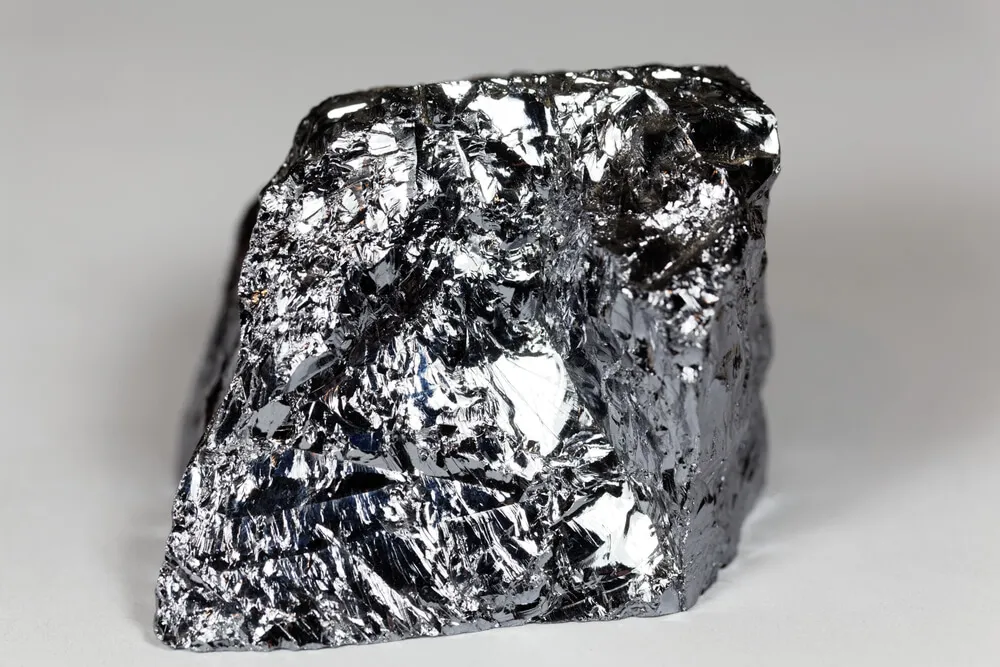
Quality begins with raw materials. Manufacturers meticulously select the purest silicon crystals to serve as the foundation for their wafers. Any impurities can compromise the overall functionality and reliability of the final product.
The selected silicon crystals undergo a process called crystal growth, where they are transformed into cylindrical ingots. The controlled growth conditions ensure a uniform and defect-free crystalline structure, which is crucial for consistent semiconductor performance.
The ingots are sliced into ultra-thin wafers using diamond saws. Precision is key here, as the thickness of each wafer impacts its electrical properties. Subsequent polishing smooths the surface to near perfection, enabling optimal circuitry fabrication.
This step involves projecting intricate circuit patterns onto the wafer's surface using photomasks. Chemical etching then removes unwanted material, leaving behind precisely defined circuitry.
Dopants are introduced into specific areas of the wafer to control the conductivity of the semiconductor. Annealing, a high-temperature process, activates these dopants and repairs any crystal damage caused during prior steps.
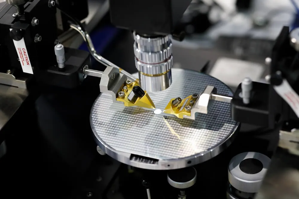
Advanced metrology tools are employed throughout the manufacturing process to measure critical parameters such as thickness, alignment, and electrical properties. Wafers also undergo rigorous testing to identify defects, ensuring only flawless components proceed.
After circuitry fabrication, individual chips are separated and packaged. Comprehensive testing, including functional, performance, and reliability assessments, is conducted on representative samples to confirm adherence to specifications.
Wafer manufacturers implement stringent quality management systems that adhere to international standards. These systems encompass various aspects, from documentation and traceability to continuous process improvement.
In the world of semiconductors, precision is paramount. Wafer World leaves no stone unturned in its pursuit of quality, leveraging cutting-edge technologies and meticulous processes to produce components that power our modern lives.
Each step in the manufacturing journey is a testament to their commitment to excellence, ensuring the semiconductor wafers driving our devices are of the highest quality possible. Call to order now!


