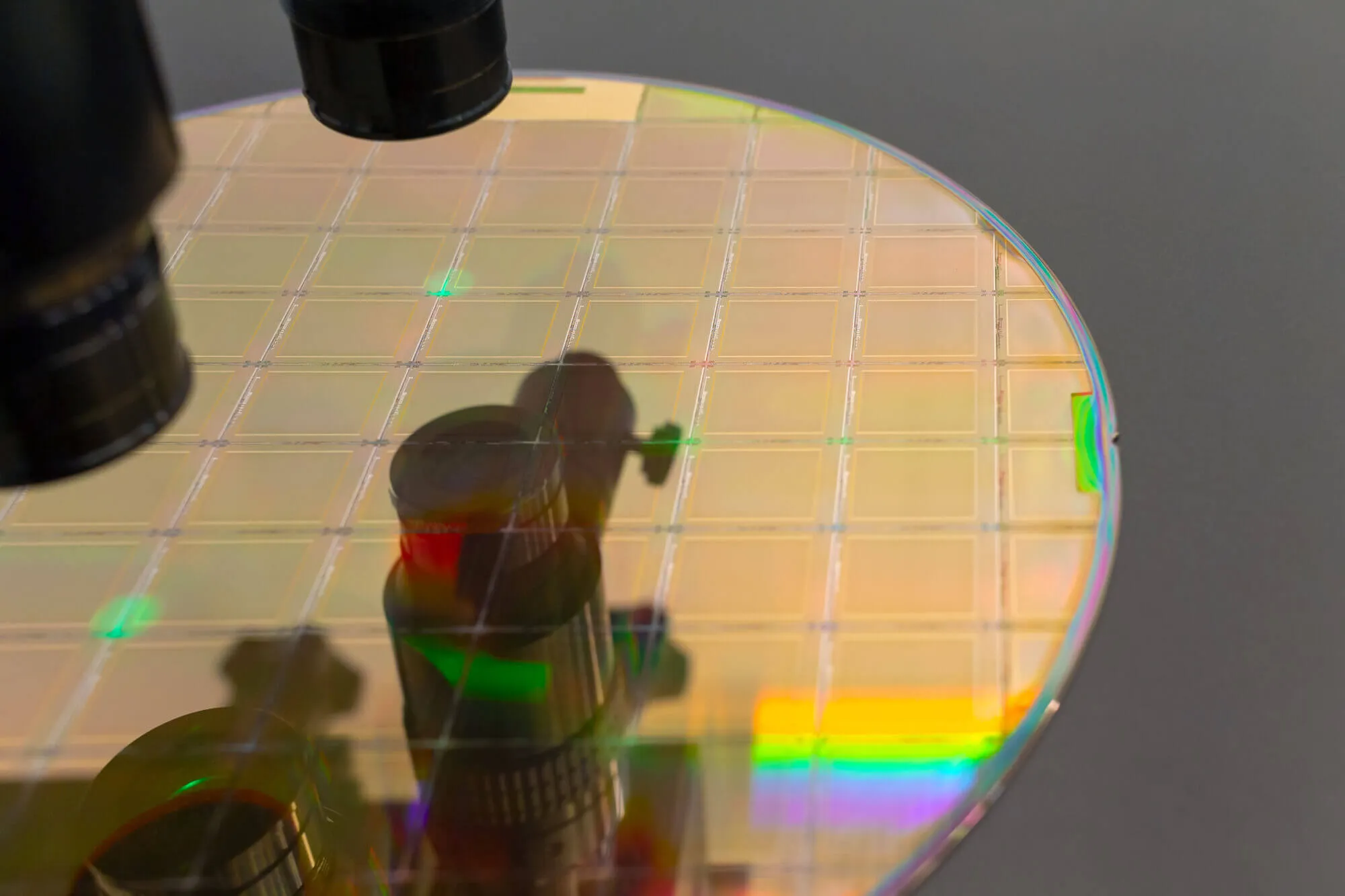
Float Zone or FZ wafers are used for detector applications due to their composition and elements. While this method is commonly used in processing silicon, the Czochralski method has also been examined in the hunt for harder materials to conduct radiation testing. If you want to learn more about these processes, here’s everything you need to know about float zone and the Czochralski method.
Silicon made from the float zone method has a high-purity substitute for crystals compared to the Czochralski procedure. While light impurities like carbon and oxygen are present in very small amounts, this doesn’t affect the overall quality of the silicon. Nitrogen, another light impurity, is now purposefully supplied during the growth stages to assist control of micro defects and improve the mechanical strength of the wafers.
They created the Float Zone (FZ) approach in 1962, based on the zone-melting theory. Production happens in a vacuum or an environment made of inert gases to help prevent impurities from forming during production. A high-purity polycrystalline rod and a mono-crystalline seed crystal are held vertically face-to-face and rotated to begin the process.
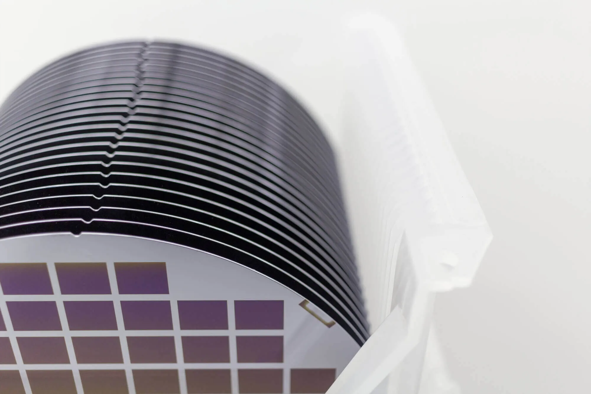
Because of the greater resistance of the wafers to thermal stress, the speed of production, the low cost, and the high oxygen concentration that allows for Internal Gettering, Czochralski silicon accounts for the vast majority of commercially manufactured silicon. The diameter of industrial standard crystals ranges from 75 to 200 mm, and they are normally l m long and 100> oriented.
The Czochralski method is named after J. Czochralski, who measured the speed at which metals crystallized by yanking mono- and polycrystals out of a melt contained in a crucible. Teal and Little created the commonly used pull-from-melt technique in 1950.
In the spinning quartz crucible, the Czochralski technique begins by melting high-purity polysilicon (SGS) with extra dopants for ultimate resistivity. A single crystal silicon seed is deposited on the surface and slowly dragged upwards while rotating simultaneously.
This attracts molten silicon, which forms a continuous crystal that extends from the seed. Temperature and pulling speed are regulated to narrow the crystal diameter to a few millimeters, eliminate dislocations caused by the seed/melt contact shock, and broaden the crystal to full diameter.
At Wafer World, our team can provide fast and reliable service to get the needed materials. Give us a call to learn more about the products we offer!


