
Wafer orientation is crucial for GaAs wafers, and selecting the incorrect orientation can significantly impact device performance, epitaxial quality, yield, and long-term reliability.
Whether you’re fabricating RF devices, optoelectronics, or compound semiconductor research structures, understanding GaAs crystal orientation is critical to getting consistent results.
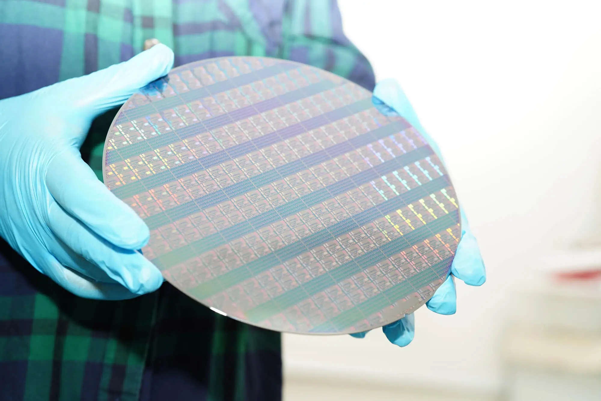
Wafer orientation refers to the crystallographic plane exposed on the surface of the gallium arsenide wafer. Common orientations are defined using Miller indices, such as (100), (110), or (111), sometimes with an intentional miscut (off-axis angle).
Because GaAs is a single-crystal compound semiconductor, its electrical, optical, and epitaxial growth behavior changes depending on how the crystal lattice is exposed at the surface.
There are three main GaAs orientations:
The right orientation depends on:
If you’re unsure, starting with (100) GaAs with a controlled miscut is often the safest and most cost-effective choice.

With GaAs wafers, orientation is not a minor specification. It directly affects growth behavior, electrical performance, and manufacturing success. Selecting the right orientation early can save time, reduce defects, and enhance the final device's performance.
Do you need help sourcing the right GaAs wafers? Reach out to Wafer World for advice from expert manufacturers!


