A wafer is a semiconductor material which is finely cut. It can be made of a silicon crystal which is used as a base in the manufacturing of microdevices and integrated circuits. This wafer goes through a series of microfabrication steps such as doping, deposition, removal, patterning, modification of electrical properties, etching, and implantation. A double side polished wafer, on the other hand, is a wafer but manufactured for a specific purpose. Wafers are rampantly used in many forms of modern technology nowadays: solar cells, circuit boards, microchips, and chips.
A wafer’s diameter or thickness is important because there are applications that have specific requirements. A double side polished wafer is compulsory in semiconductors, MEMS, and other application that is strict towards the thinness of the wafer. They are also significant for double side patterning and device fabrication projects. Today’s trend of a slimmer, compact and smaller technology forces semiconductors to shrink its size. But is not an excuse to sacrifice the high surface quality of the wafer. As of now, it is rampantly used in microelectromechanical systems, wafer bonding, silicon on insulator (SOI) manufacturing, and applications with strict thinness standards.

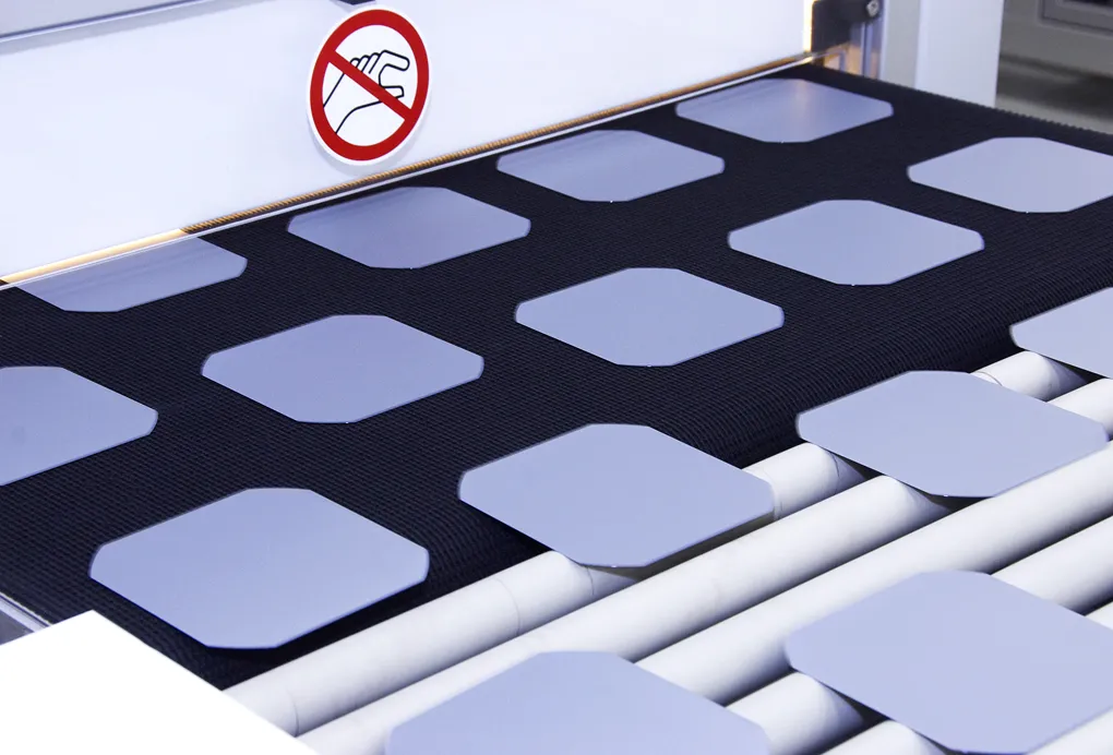
If you need a quality double side polish wafer for your next project, then contact us today. At Wafer World, we offer only the purest of quality wafers for your needs. You can reach out to us and discuss what wafer suits your project best. You can request a quote by filling out a form on our website and we will reach out to you as soon as possible.


