A double side polish wafer can look like a standard wafer that simply got extra attention. Both faces carry the same mirror-like finish, while a single-side polished (SSP) wafer has only one finished surface and a rougher back.
But the second polish isn’t cosmetic. By removing the damaged layers left from slicing and lapping, double side polishing improves flatness and thickness uniformity, which makes it essential for applications that depend on two reliable working surfaces.

Ingots are sliced, ground, and cleaned to produce wafers, and that process leaves a damaged layer near the surface, sometimes only a few microns deep, that can affect wafer quality and performance if left unaddressed.
Polishing removes that layer. Doing it on both sides, rather than just the front, improves the wafer's overall flatness and gives it the mirror finish that minimizes roughness and reduces particle trapping during later processing.
That polishing step typically follows lapping and grinding, which bring the wafer close to its target thickness and correct gross irregularities. Polishing then refines the surface further, removing the fine subsurface damage those earlier steps leave behind.
The sequence matters: polishing works best as the final refinement on a wafer that already has reasonably controlled geometry, not as a way to correct major problems introduced earlier in the process.
Not every application needs both sides polished. Standard CMOS and IC fabrication typically only use the front surface for photolithography and doping, so the backside adds little value from polishing.
Double side polishing earns its cost in wafer bonding and double-sided lithography, MEMS fabrication that requires etching or alignment from both faces, silicon-on-insulator production, and high-precision optical applications where both surfaces matter to the finished device.
Not necessarily. For applications that only use the front surface, single-side polished wafers perform the same job at a lower cost. Double side polishing is worth the added expense specifically when both surfaces play a functional role.
It can reduce gettering capacity, the wafer's ability to trap unwanted metal impurities away from active circuit areas, since that capacity is often tied to the unpolished backside of a single-side polished wafer.
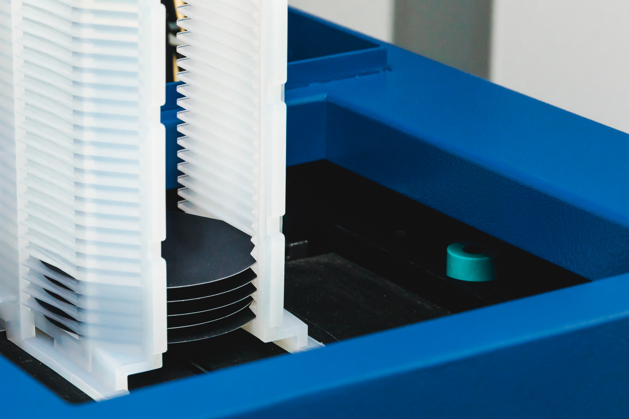
Choosing between single and double side polished wafers comes down to whether your process actually uses both surfaces. Wafer World maintains stock across both options to support quick turnaround. Request a quote and the team can help confirm which specification fits your application.