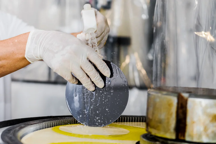
Wafer geometry can influence what happens long after a substrate leaves the polishing stage. When thickness changes noticeably from one area to another, subsequent equipment may encounter differences in support, focus, contact, or measurement conditions. A double side polish wafer addresses this concern by refining both major surfaces as part of a controlled finishing process.
Rather than treating surface quality as an isolated cosmetic characteristic, double-side polishing contributes to the broader goal of producing a substrate with controlled geometry, smooth surfaces, and consistent thickness. Understanding how the process affects thickness variation helps engineers evaluate wafer quality more meaningfully before substrates move into demanding fabrication steps.
Thickness variation describes differences in wafer thickness across its usable area. It is not simply the nominal thickness printed on a specification sheet. Two wafers can have similar average thicknesses while showing different thickness distributions from point to point. That distinction matters because semiconductor manufacturing depends on repeatable relationships among the wafer, process equipment, and the features formed on its surface.
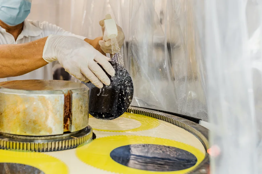
A wafer with better thickness uniformity provides a more predictable physical starting point. During processes that rely on controlled positioning or surface geometry, local differences can influence how the substrate behaves. The importance becomes clearer when considering photolithography, inspection, bonding, and other processes in which wafer geometry can affect alignment or measurement.
The National Institute of Standards and Technology has studied total thickness variation, commonly called TTV, using interferometric methods. This work reflects the importance of evaluating thickness across the wafer rather than relying solely on a single-point measurement.
Nominal thickness indicates the intended or representative thickness of a substrate. TTV focuses on the difference between thicker and thinner regions across the measured wafer area. As a result, meeting a nominal thickness target does not automatically mean that the thickness is equally consistent everywhere.
This distinction is useful during wafer evaluation. A substrate may fall within an acceptable overall thickness range yet still contain localized variations that matter for a particular process. Considering both nominal dimensions and spatial uniformity gives engineers a more complete picture of the substrate geometry.
Double-side polishing s designed to remove material from both wafer faces. That basic arrangement has an important geometric advantage: both surfaces can be refined relative to each other rather than treating one finished surface independently of the unfinished opposite side.
Before polishing, earlier manufacturing steps have already shaped the substrate. Slicing creates the initial wafer, while subsequent lapping, grinding, or etching can remove damage and bring dimensions closer to target conditions. Polishing then provides additional surface refinement and flatness control.
The Semiconductor Industry Association describes wafer refining as a sequence in which double-side grinding or lapping improves flatness and moves thickness closer to specification, followed later by polishing that removes surface damage, improves flatness, and creates a mirror-like finish. This sequence shows why thickness control is the result of coordinated processing rather than one isolated operation.
Material removal during polishing must be controlled across the wafer area. If removal is disproportionately concentrated in certain regions, the final substrate can develop unwanted thickness differences. Processing both faces provides another way to manage the relationship between the two surfaces during wafer finishing.
Several variables can influence the result, including polishing pressure, pad condition, slurry behavior, wafer motion, process time, and the geometry entering the polishing step. These factors must work together. Polishing cannot fully compensate for issues arising during earlier manufacturing stages, which is why the incoming wafer condition remains important.
Flatness and thickness variation are sometimes discussed as though they describe the same characteristic. They are connected, but they answer different questions. Thickness variation concerns the distance between the two wafer surfaces at different locations. Flatness concerns the shape or deviation of a surface relative to a reference condition.
A wafer can therefore require evaluation through multiple geometry measurements. NIST research on silicon wafer metrology has specifically addressed both thickness variation and flatness, including measurements of free-standing and chucked wafers. Keeping these concepts separate helps prevent a single metric from being used as a substitute for a broader geometry assessment.
When both surfaces have been polished, optical measurement methods can take advantage of reflections or transmission involving the front and back surfaces. NIST has documented infrared interferometry for measuring thickness variations in double-side polished silicon wafers.
This illustrates another practical benefit of controlled surface finishing: polished surfaces can support sophisticated characterization methods. Measurement, however, remains a separate part of quality control. Polishing creates the physical condition, while metrology verifies whether that condition meets the relevant requirements.
Thickness consistency does not begin when a wafer reaches a polishing tool. Earlier steps establish the geometry that the polishing stage receives. Slicing, edge treatment, lapping or grinding, and chemical etching can all influence the condition of the substrate before final surface finishing.
A well-managed process, therefore, considers the entire sequence. SUMCO, for example, describes wafer processing as progressing through slicing, lapping, etching, polishing, cleaning, and inspection. Its process information notes that lapping is used to make both sides parallel and bring the wafer to the specified thickness. At the same time, polishing produces a highly flat mirror surface.
That progression highlights an important point: polishing works best as part of a controlled manufacturing chain. Attempting to correct substantial upstream geometry problems only at the final stage can make it more difficult to achieve consistent results.
A useful wafer assessment looks beyond whether the surface appears shiny or visually clean. Mirror finishing is important, but visual appearance alone cannot establish thickness uniformity or overall geometric performance.
Depending on the application and agreed specification, evaluation may consider several characteristics:
The appropriate combination depends on how the substrate will be used. A research environment, device fabrication line, optical application, or bonding process may place different emphasis on individual geometry characteristics. Clear specifications help suppliers and users evaluate the same requirements rather than relying on broad descriptions such as "flat" or "high quality."
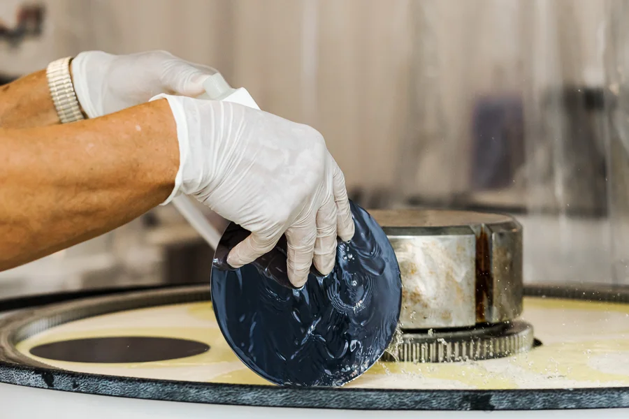
Thickness uniformity across the central wafer area does not mean the edge should be ignored. NIST measurements of polished silicon wafers have documented edge roll-off, demonstrating that wafer geometry can change near the perimeter.
This is one reason measurement definitions and exclusion zones matter. A reported value is most useful when the measurement area and methodology are understood. Comparing numbers generated under different conditions without considering those details can create misleading conclusions about actual wafer performance.
Semiconductor fabrication involves repeated interactions between a wafer and highly controlled equipment. The Semiconductor Industry Association notes that metrology is used throughout chipmaking to verify characteristics such as wafer thickness, alignment, and feature dimensions. Consistent incoming geometry gives these downstream processes a more controlled starting condition.
That does not mean polishing alone determines manufacturing yield or device performance. Many other variables contribute, including material properties, contamination control, process recipes, equipment condition, and device design. Instead, thickness uniformity should be viewed as one foundational aspect of substrate quality.
Better control of the starting wafer can reduce one source of unwanted variation. For engineers troubleshooting a process, eliminating unnecessary substrate variability can also make it easier to distinguish wafer-related effects from issues originating elsewhere in the fabrication flow.
There is no single geometry requirement that applies equally to every wafer and every use case. The appropriate substrate depends on material, diameter, orientation, device process, equipment, and customer-defined tolerances. For that reason, purchasing decisions should be based on documented requirements rather than assumptions about what polishing automatically guarantees.
Before specifying a wafer, teams can identify which measurements are critical, how those measurements are defined, and which tolerances are compatible with downstream processing. This approach makes conversations with suppliers more productive and helps prevent unnecessary over-specification.
It also encourages a more useful question than simply asking whether a wafer is polished on both sides. Engineers can ask which geometric characteristics have been measured, which inspection methods were used, and whether the resulting wafer is appropriate for their process.
TTV indicates the difference between maximum and minimum thickness within a defined measurement area. It helps describe how consistently the spacing between the wafer's two major surfaces is maintained across that area. The measurement should be interpreted alongside the applicable test method, edge exclusion, and other geometry specifications.
No. Polishing is an important part of controlling surface condition and geometry. However, final flatness depends on the complete manufacturing process and its controls. Incoming geometry, polishing conditions, handling, measurement methods, and other factors can influence the finished wafer. "Perfect" flatness should not be assumed without measured data.
Metrology verifies whether the processing produced the intended result. Thickness variation, flatness, and surface inspection provide quantitative information that visual observation cannot supply. Measurement data also helps manufacturers identify process trends and confirm whether wafers satisfy defined acceptance requirements.
Yes, depending on the application and severity of the variation. Processes involving precise positioning, focusing, bonding, or dimensional control can be sensitive to wafer geometry. The acceptable level should be determined by the specific fabrication process and its documented requirements rather than by a universal threshold.
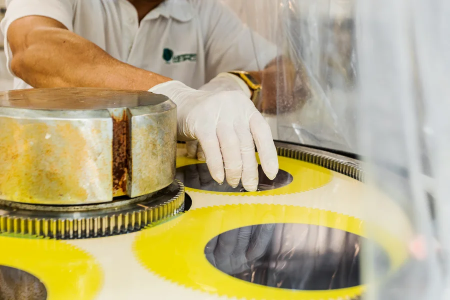
Selecting a double side polish wafer is ultimately about matching the substrate geometry and surface condition to the needs of the intended process. Wafer World can help you discuss available wafer options and the specifications relevant to your application without treating one polishing characteristic as the whole quality picture.
Contact us to schedule a consultation and review your substrate requirements before planning your next order.




