The current chip shortage has forced electronic device manufacturers and chip makers to hoard ultra thin wafers. However, most of these semiconductors are not put to use right away. Instead, they are placed in long-term storage.
Wafers are not labeled with expiry dates upon completion. Still, they could lose effectiveness if some concerns from manufacturing to storage are not adequately addressed. However, with proper storage and handling, unused wafers could be kept within controlled conditions for 18 months and still retain optimal performance.
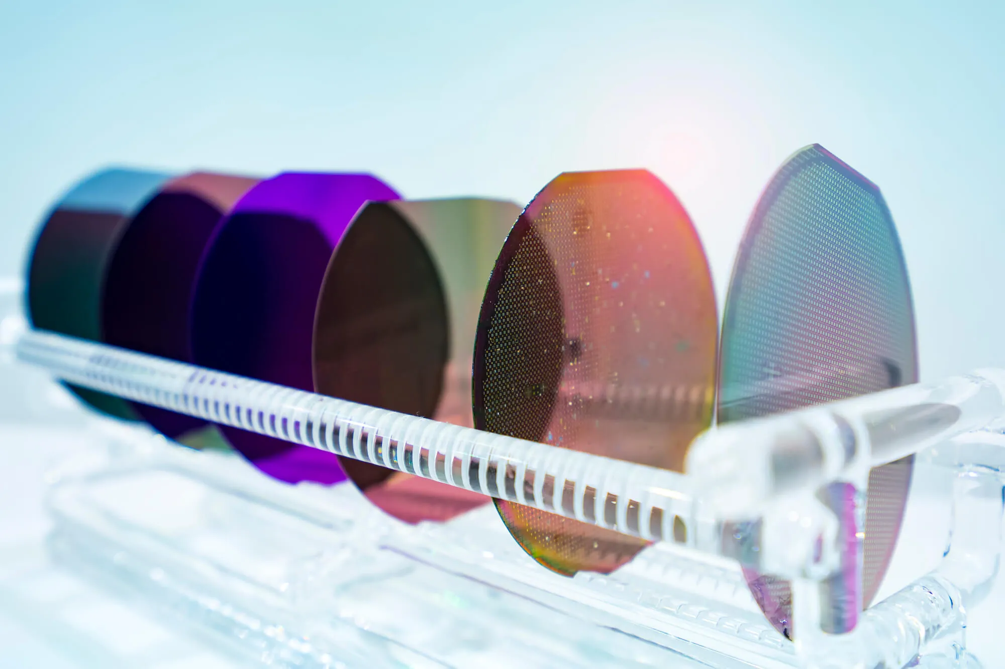
To extend the shelf life of new ultra thin wafers, manufacturers and their customers should note the following concerns during production, delivery, and storage:
Semiconductors are sensitive to electrostatic discharge. The term refers to the release of electrostatic energy resulting from contact between two objects or surfaces. ESD events include the connection between a doorknob and someone who has just walked across a carpet, or a lightning strike.
These events differ in intensity, but they have one common denominator: a transfer of electricity and heat. Humans may feel nothing more than a mild shock, but electronic devices can sustain enough damage from the heat to cause failure. For example, the discharge could burn through the miniature gates and spike contacts in chips.
When handling virgin wafers, wafer fabricators and their clients must minimize or avoid static electricity accumulation. Team members must also wear devices that divert any electrostatic discharge to the ground away from the device.
Moisture is a significant risk to wafer health during storage. Parts of the wafer can be easily corrupted by moisture, like the hardened photoresist and the semiconductor itself. That is why manufacturers build chips onto wafers in a controlled environment where humidity is kept at a certain level and is not allowed to exceed specific thresholds.
Humidity changes with temperature and temperature shifts can cause a temporary accumulation of static electricity through the pyroelectric effect. On the other hand, a more stable environment keeps the conductivity level balanced, so there is no electrostatic accumulation that could discharge and damage any circuits in the wafer and attached dies.
Antistatic packaging achieves the same environmental control as cleanrooms when transporting wafers from the production facility to the customer’s storage spaces.
As chips become smaller, the effects of contamination on wafer performance and production yield become more significant.
Surface contamination comes from organic and inorganic sources that the wafer comes into contact with during production. For instance, the Czochralski method can leave some impurities when the crucible melts and bonds with the grown silicon ingot. The same effect occurs during doping, which introduces atoms to the molten silicon to manipulate its conductive capabilities.
Wafers can also contact inorganic chemical contaminants if the cleanrooms have exhaust and airflow issues. Moisture can turn parts of a Si wafer into silicon oxide. This atomic setup will degrade the silicon’s performance or make it unusable.
Fortunately, a strict QA process can vet out contaminated wafers. Quality control personnel can decide whether to discard the product or reclassify them into test-quality output. Extra care should be taken when storing test wafers because their existing imperfections can worsen in the improper storage environment.

As indicated above, the quality control process is the barrier that prevents the delivery of fatally flawed wafers to the customer. Current QC technologies employed in wafer production are optical, however, and still have limitations and margins of error.
The OPWI system uses a scanner to map out the surface of the wafer. Afterward, the operator superimposes the image against a circuit diagram. Alternatively, they use a “perfect” chip as a reference image to compare and detect flaws.
The EBI uses an electron gun and a detector lens system to generate a wafer’s high-resolution image. Like the electron microscope, the EBI can magnify samples up to 1 nanometer. Due to its slow image generation, the system primarily scans specific portions of the wafer for defects.
Wafer QA is one of the possible applications for terahertz imaging technology. It uses light waves in the 100 GHz-10 THz range and extremely short wavelengths to survey and create a picture of a specimen.
All three technologies are still subject to human fatigue and error. Their effects in QA are more pronounced when scanning processors due to the increasing number of nodes in new-generation sets.
Wafers require special packaging that keeps them free from damage. There are multiple options for wafer delivery packages, and these are:
Like the old tape cassettes, wafer cassettes provide a sturdy plastic housing for multiple wafers. The package keeps each wafer from coming into contact with each other during travel. Because of convenience, both untested and tested wafers can be packed in this option.
Carrier boxes provide insulation for each individual wafer the same way cassettes do. However, unlike cassettes, wafers must be extracted from the box for post-processing and returned after the process. This condition provides an opportunity for contamination from the external environment.
Waffle packs are specialized plastic trays with embossed spaces matching the dies in a multi-project wafer. Manufacturers select this option when the delivery volume is less than the minimum number of wafers that fit in a cassette.
Waffle packs keep out contamination through an antistatic bag and an airtight lid. However, they don’t keep the wafers from touching the case’s edges during transit.
Gel packs use surface tension to keep the dies in place even when the container tilts or is flipped on its back during transit. This packaging minimizes the chances of the wafers rubbing against each other and sustaining scratches on their surfaces.
.jpg)
All of our wafers are manufactured in a process that maximizes production yields. We also work with various types of semiconductors. Contact us now and find out more about our products.


