
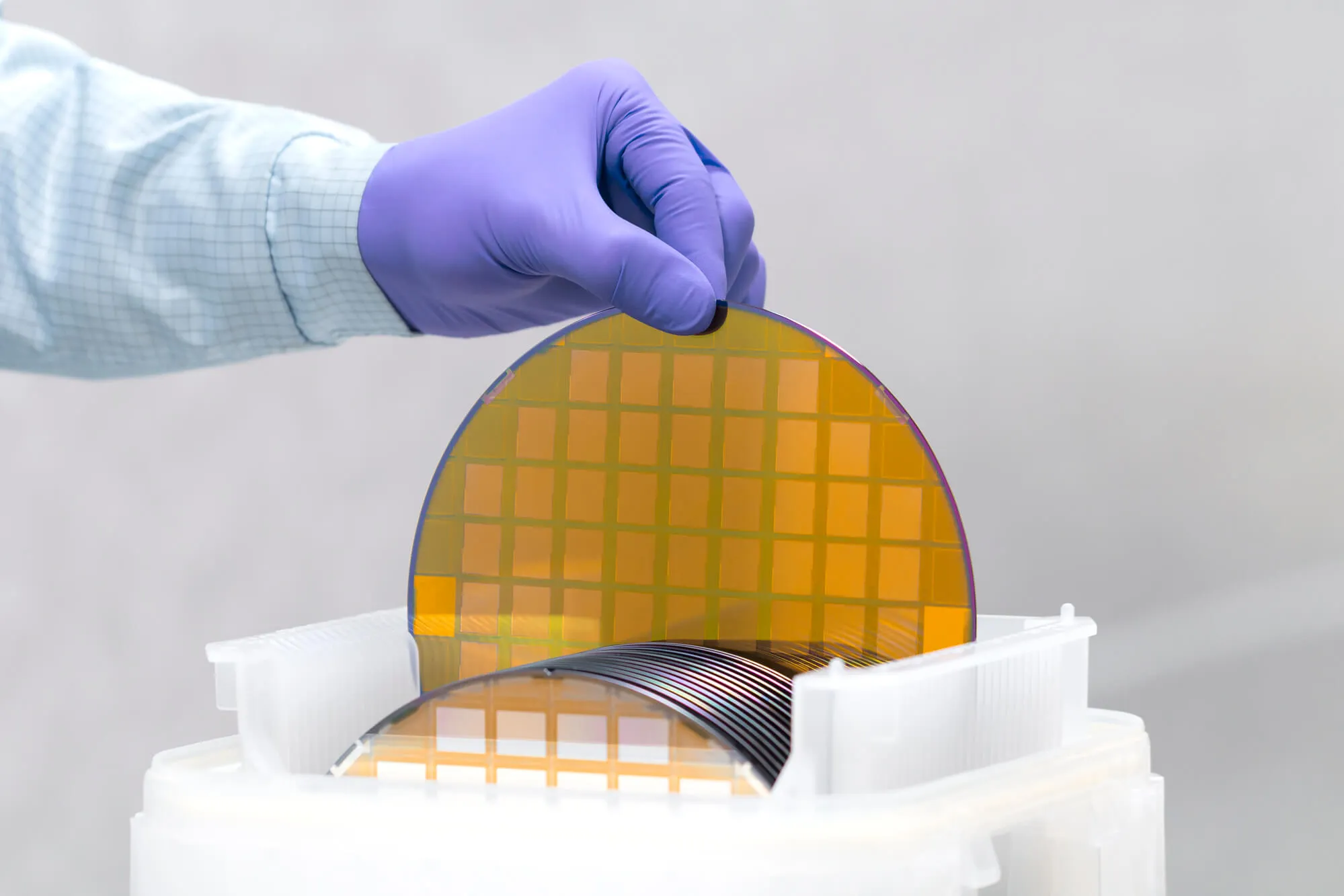
As we’ve discussed extensively on this blog, there are a wide range of wafers that can be used for semiconductor production, and the choice of which one you get can have major ramifications on the product that your client creates.
While it’s common to use silicon when manufacturing wafers, this is actually one of just many potential materials available. The architecture used for the semiconductor, as well as concerns about supply chains, can all determine what the wafer you want will actually look like.
Today, we’ll discuss everything you should know when determining which wafer you want.
https://www.youtube.com/watch?v=O9zH3fd24K4&ab_channel=WaferWorldInc.
As you likely know, wafers are essential for the creation of semiconductors. And given their name, semiconductors all have semi conductivity in common. In certain situations, they will conduct energy. In others, they won’t.
That said, beyond this basic fact, the wafer material you choose can have a major impact on the capabilities of your semiconductor. These materials have varying levels of cost, ability, durability, and more.
Here are a few of the most common materials.
Silicon is the most common wafer material, which makes sense, because it’s also one of the most abundant elements in the universe.
Many companies choose silicon because it’s so popular and easy to work with, and its ubiquity and versatility often make it a great choice if you need a semiconductor.
That said, it’s important to consider different use cases. Often, you can increase the efficiency or power of your product by making sure you’ve chosen the best material for your needs, as opposed to choosing silicon without considering your other options.
If you’re unsure which material you need, it’s always a good idea to partner with a trustworthy wafer supplier with significant experience in the industry. They can help point you in the right direction, using their experience to help you find exactly what you need.
Funnily enough, germanium was used as a semiconductive material before silicon. That said, this is no longer the case. While it is actually similar to silicon in many ways, it’s more sensitive to gamma radiation.
For this reason, it’s often used for photodetection. Here are a few examples of products that might benefit from germanium wafers:
Gallium Arsenide is a versatile, cost-effective semiconductor material. It’s important for its ability to be repurposed: it’s possible to “reclaim” the GaAs to use it again for a different purpose.
Along with being more cost-effective, reclaimed wafers are also great because of their eco-friendliness.
Here are just a few of the potential applications of reclaimed GaAs wafers:
Sapphires are an excellent choice for all kinds of wafers. It's a nine on the Mohs scale, which means it’s extremely hard to break. It’s also resistant to a variety of harsh conditions, such as heat or chemicals.
Of course, sapphire is an expensive material, which is why it’s not often used for consumer applications. That said, there are all kinds of potential applications for sapphire wafers, including:
Along with being used in certain civilian cases, it’s a popular material for military uses.
Indium Phosphide (InP) is an extremely powerful and durable material, which means it’s often used in delicate situations that require high performance. Its direct band gap and high electron mobility make it excellent for the following use cases:
Much like GaAs wafers, InP wafers can also be reclaimed.
Of course, in the perfect world you’d be able to use all the materials you want to build your semiconductor. However, the past several years have shown us that we do not live in a perfect world.
The classic example of this is the difficulties that arose when trying to get semiconductor during the COVID-19 pandemic. China’s policy of locking down borders and shutting down production whenever a single case was found made it extremely difficult to receive goods from the country.
This was problematic because Taiwan supplies many of the semiconductors that power the rest of the world.
Even world events that wouldn’t seem to have any impact on semiconductor productions have completely changed the ability to produce semiconductors. The war between Russia and Ukraine is a perfect example of this.
Neither country is a major supplier of semiconductors, and neither of them holds resources essential for the creation of semiconductors. In fact, silicon being one of the most abundant elements means that it would be extremely difficult for any one country to hold a monopoly on its production.
That said, Ukraine is a major supplier of neon, which is used to draw patterns on wafers. While this seems like a small element of the process, it’s an essential one, and it means that the Ukraine-Russia War has impacted the supply of semiconductors.
Luckily, in many situations you’re not restricted to only a single kind of semiconductor. That said, if you’re unable to get a material and need to go through the design process again, you may need to spend a lot of money and a lot of time.
When you’re initially designing a wafer, it’s a good idea to make sure you can get as much of what you need domestically as possible. In fact, that’s also why we recommend that US semiconductor companies work with US wafer manufacturers: you don’t have to worry about the logistics of international shipping.
.webp)
You’ve come to the right place. At Wafer World, we partner with semiconductor companies to ensure they have the wafers best suited to their needs. With over 30 years of experience in the industry, combined with a commitment to always staying on the cutting edge, you can rest easy knowing you’re in good hands.
Do you have any questions about what we can do for you? Would you like to speak with a wafer expert? Please don’t hesitate to reach out to us! We’re excited to speak with you.


