FZ wafers are essential to the production of high-performance semiconductors, but many consumers struggle to find organized, trustworthy, and clear information about them. Understanding the entire environment surrounding FZ wafers is crucial to comprehending, assessing, and confidently choosing the best wafer for your project.
Whether you're looking for high-resistivity wafers for RF devices, ultra-pure silicon for sensors, or custom doping profiles for power electronics, this glossary offers simple definitions, technical insights, and practical guidance—all in one place.
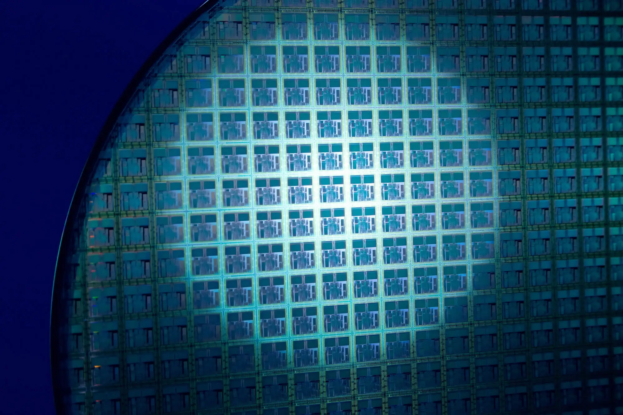
FZ wafers, also known as float zone wafers, are single-crystal silicon wafers made using the Float Zone Method, which is renowned for producing the purest silicon in commercial quantities. A crucible is not used in FZ manufacturing, unlike the Czochralski (CZ) method.
Because of this, oxygen contamination is eliminated, and impurities are significantly reduced, making FZ wafers perfect for applications that need:
If your device relies on clean, stable, and high-performance silicon, FZ wafers are often the top choice.
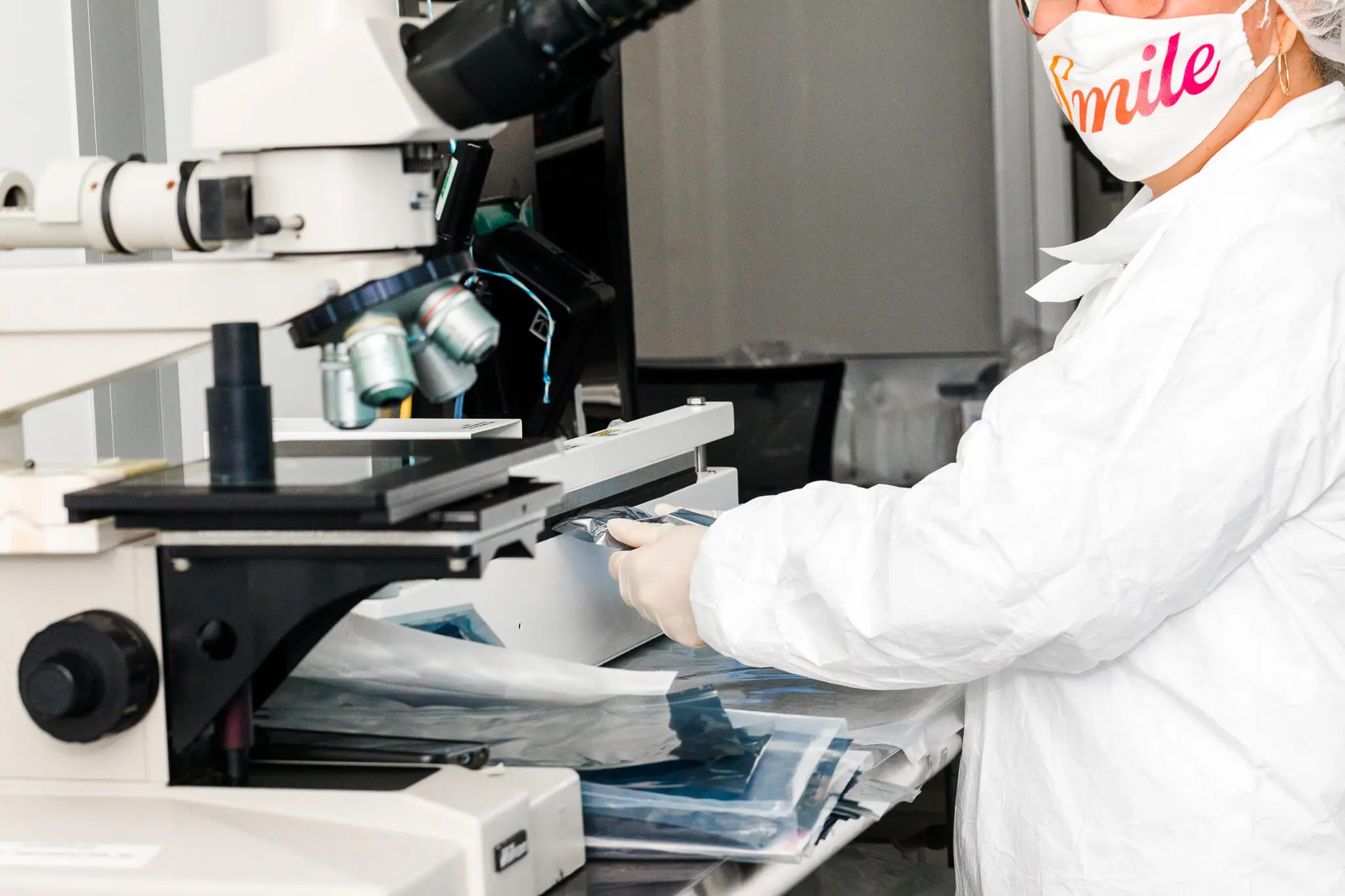
To make consistent, reliable decisions, engineers, researchers, and procurement teams need clean, authoritative references on FZ wafers. Here are some key terms related to Float Zone (FZ) silicon wafers, including the growth method, materials involved, and characteristics that are crucial in semiconductor research and manufacturing.
The minimum energy needed to activate carriers or impurities in silicon. In FZ wafers, low contamination levels result in more predictable activation behavior.
A controlled heating process is used to repair lattice damage or activate dopants. FZ wafers, thanks to their low defect density, often require shorter or more precise annealing treatments.
The amount of time charge carriers (electrons or holes) remain mobile before recombining. FZ wafers offer extremely high carrier lifetimes because of their minimal impurity levels.
The amount of carbon impurities present in silicon. The Float Zone process naturally minimizes carbon, improving purity and electrical performance.
A common method for growing silicon uses a quartz crucible. Unlike FZ, it introduces oxygen into the crystal. CZ is often used for cheaper, lower-resistivity wafers.
The atomic alignment of the silicon lattice is expressed in terms of Miller indices, such as <100>, <111>, or <110>. Orientation determines mechanical, electrical, and etching properties.
The number of crystal imperfections per unit area or volume. FZ silicon offers some of the lowest defect densities among all wafer types.
The intentional addition of impurities like boron, phosphorus, or arsenic to alter electrical conductivity. FZ wafers support precise doping control across a wide range of resistivities.
A surface finish where both sides of the wafer are polished to near-perfect flatness and reflectivity. Common for optical and measurement applications.
The shape and contour of the wafer’s outer edge typically follow SEMI standards (e.g., beveled or rounded). Proper edge profiling reduces breakage during processing.
A crucible-free silicon growth process where a molten zone is “floated” upward through a polycrystalline rod. This method removes impurities and yields ultra-pure single-crystal silicon.
The speed at which the single-crystal ingot grows during the Float Zone process. A slower rate typically reduces defects and improves uniformity.
Silicon engineered to achieve resistivity levels above 1,000 Ω·cm, often exceeding 10 kΩ·cm. This is a key benefit of FZ wafers and essential for RF, microwave, and detector applications.
A solid cylindrical block of high-purity silicon from which wafers are sliced. FZ ingots exhibit extremely low oxygen and defect content.
Silicon with low concentrations of dopants is often used in detectors or high-voltage devices. FZ silicon is ideal for maintaining uniformity in lightly doped regions.
A key performance indicator for detectors and photovoltaics, defining the persistence of minority carriers. FZ wafers typically offer exceptionally high values.
Silicon doped with electron-donating elements such as phosphorus or arsenic. Common in high-voltage and RF applications.
A defining property of Float Zone wafers. Since no crucible is used, the ingot contains virtually no oxygen impurities, which reduces defects and improves its electrical behavior.
Silicon doped with boron to create hole-based conduction. Used in sensors, detectors, and several power devices.
A wafer whose surface is finished to an extremely smooth, mirror-like state. FZ wafers can be single-side polished (SSP) or double-side polished (DSP).
The measure of how strongly silicon resists electrical current. FZ wafers feature highly controlled and uniform resistivity ideal for high-frequency and high-voltage devices.
A measure of the consistency of resistivity across the wafer surface. The Float Zone method produces excellent uniformity, especially in high-resistivity ranges.
A post-slicing process involving chemical etching to eliminate microcracks and damage caused by the cutting process.
Silicon has one continuous crystalline structure. FZ wafers represent one of the purest forms of single-crystal silicon available.
A surface finish where only the front side is polished. Common for device fabrication, where back-side polish is not required.
The ability of silicon to conduct heat. FZ wafers typically offer superior thermal conductivity, important for high-power devices.
The acceptable variation in wafer thickness across its diameter. FZ wafers are available with standard or customized tolerances.
Silicon with extremely low levels of metallic and oxygen contamination. Float Zone growth is the preferred method for achieving ultra-high purity.
The slight curvature of a wafer is measured as deviation from a flat plane. Lower bow improves lithographic accuracy; FZ wafers typically perform well in this area.
Metrics that describe the uniformity of the wafer surface. Uniform flatness is essential for advanced lithography and bonding.
A flat or notch on the wafer edge is used to identify orientation and doping type during processing.
SEMI standards usually specify the vertical dimension of the wafer. FZ wafers can be manufactured in standard or customized thicknesses.
A purification technique used in conjunction with the Float Zone process, in which the molten region carries impurities upward and away from the crystal growth area.
FZ wafers deliver unmatched purity, stability, and performance—making them the preferred choice for applications where device efficiency, sensitivity, and reliability cannot be compromised.
If you’re still unsure about whether or not FZ wafers fit your project’s needs, Wafer World can help. Whether supporting advanced research, high-precision sensors, or high-voltage devices, our FZ wafers provide the most reliable and highest-performing platform available. Contact us today for more information!


