When selecting the right silicon substrate for advanced semiconductors, understanding the differences between Czochralski-grown and FZ wafers is essential. Material choice directly impacts device reliability, breakdown voltage, switching efficiency, and long-term stability.
For engineers, researchers, and procurement teams, the decision is rarely about cost alone. It is about performance, consistency, and application fit.
In high-performance microchips, especially those used in power electronics and RF systems, subtle material differences can determine overall device success.
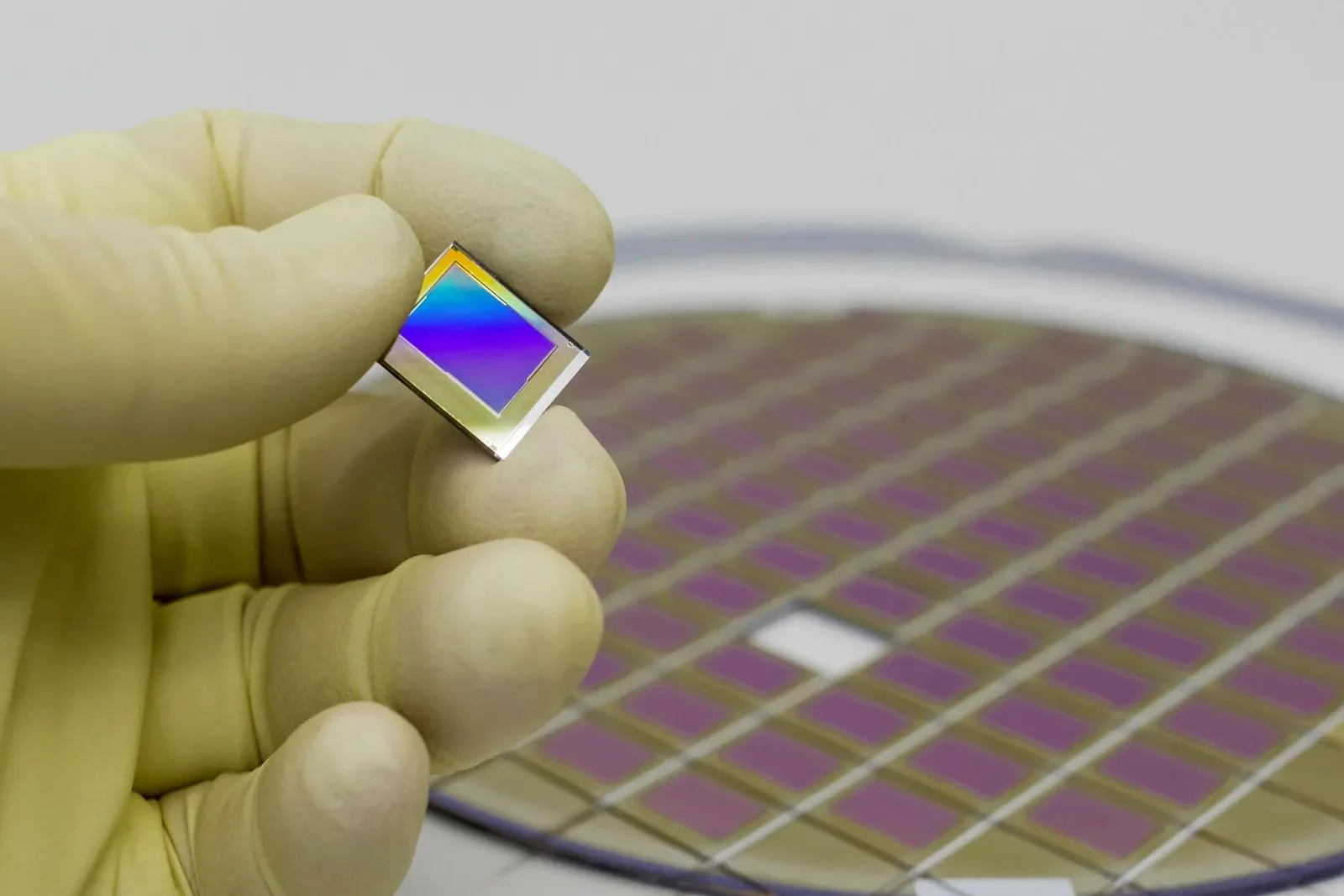
Silicon wafers begin with crystal growth. The method used defines oxygen concentration, impurity levels, and defect density, all of which affect device behavior.
The Czochralski method involves pulling a single-crystal ingot from molten silicon in a quartz crucible. During the process, oxygen from the crucible dissolves into the melt and becomes incorporated into the crystal lattice.
CZ silicon is widely used because it allows large-diameter ingots, consistent production, and cost efficiency. It is common in logic devices, memory, and general semiconductor manufacturing.
However, the oxygen content, while beneficial in some mechanical aspects, can limit performance in certain high-voltage and high-frequency applications.
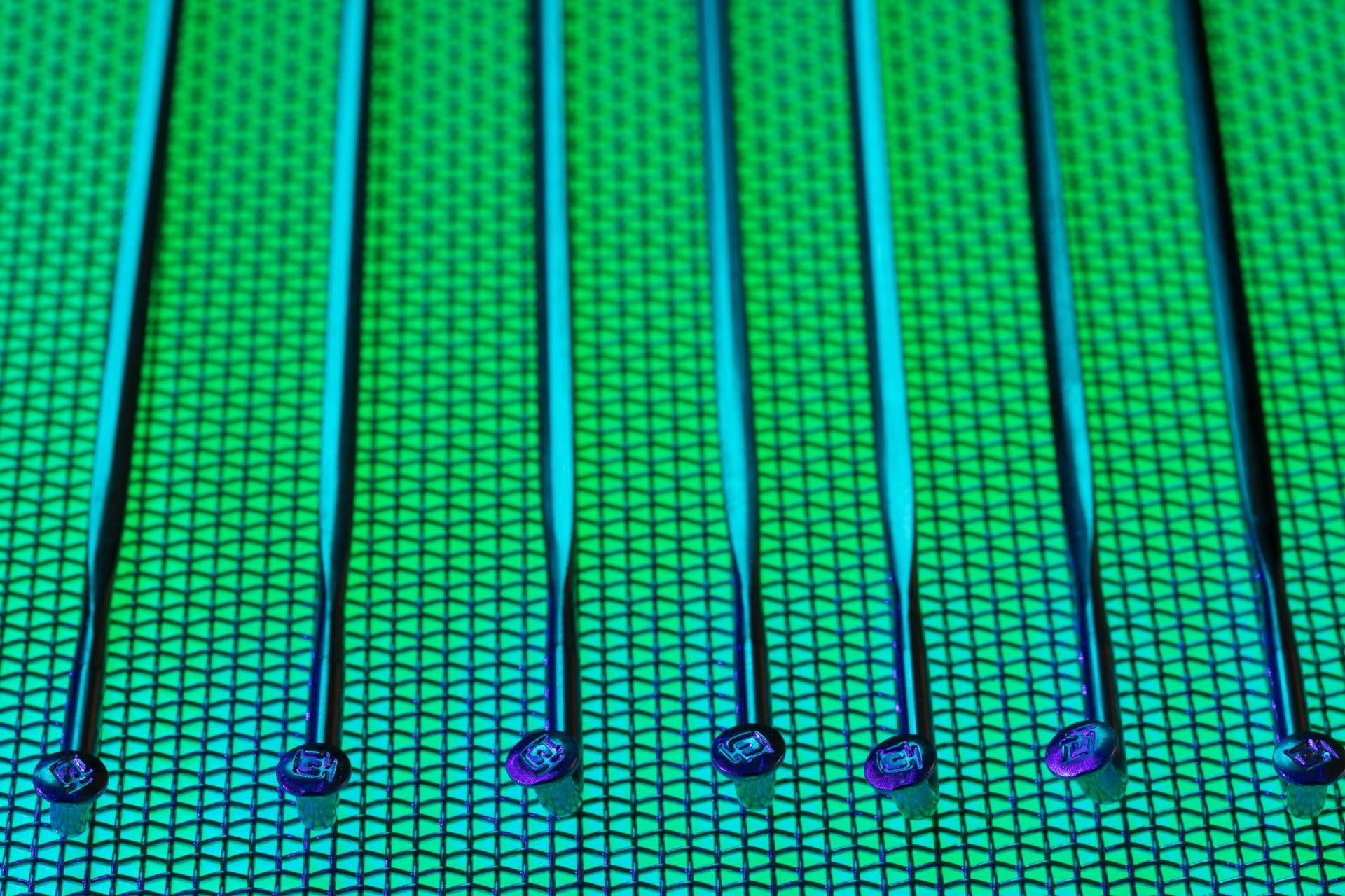
The float zone method avoids a crucible entirely. Instead, a localized molten zone passes along a vertically mounted silicon rod. As it moves, impurities are segregated and reduced, resulting in extremely high-purity material with very low oxygen concentration.
This is where the FZ wafer stands apart. Because it is not grown in contact with a crucible, oxygen contamination is minimal. That purity becomes critical in demanding power and RF environments.
One of the most significant differences between these two wafer types is oxygen concentration.
In CZ silicon, oxygen can improve mechanical strength and help control certain types of crystal defects. For many standard applications, this is acceptable and even beneficial.
However, in high-voltage devices, oxygen can form thermal donors or precipitates under certain thermal cycles. These defects may influence carrier lifetime, leakage current, and long-term stability.
The float zone process produces silicon with extremely low oxygen levels. This results in improved resistivity uniformity and fewer unwanted defects during device fabrication.
For applications such as IGBTs, high-voltage MOSFETs, and RF power transistors, this material advantage can directly affect performance margins and reliability targets.
Resistivity is a defining specification in semiconductor substrates.
Float-zone material supports very high, tightly controlled resistivity levels. This makes it particularly suitable for:
An FZ wafer is often selected when breakdown voltage and carrier lifetime must be carefully managed.
Czochralski silicon can also be produced over a range of resistivities, but the presence of oxygen and thermal donors may introduce variability under certain processing conditions. For many standard integrated circuits, this is not a limiting factor. For specialized power devices, it can be.
Crystal defects influence recombination rates, leakage currents, and switching behavior.
The float-zone process yields lower impurity concentrations, such as carbon and oxygen. This often results in longer minority carrier lifetimes, which are essential in many power semiconductor devices.
Longer carrier lifetime contributes to:
These characteristics are critical in electric vehicles, renewable energy inverters, and industrial motor drives.
While CZ wafers are mechanically robust and cost-effective, oxygen precipitates formed during high-temperature processing can create defect clusters. Device designers must account for this in process integration and reliability modeling.
Wafer size impacts manufacturing scalability and cost structure.
Czochralski silicon is more commonly available in very large diameters. This supports high-volume manufacturing and cost efficiency in consumer electronics and mainstream microchips.
Float zone ingots are generally smaller in diameter due to process constraints. For many high-performance applications, the performance benefit outweighs the size limitation. Choosing between the two often depends on balancing performance requirements with manufacturing scale.
Selecting the appropriate substrate depends on device type and performance expectations.
High-voltage and high-current devices often use float-zone material due to its superior resistivity control and low oxygen content. These attributes support higher breakdown voltages and improved reliability under electrical stress.
High-resistivity silicon is often preferred for RF components to minimize substrate losses. In such cases, an FZ wafer provides electrical isolation, enhancing signal integrity.
For mainstream logic devices and memory chips, CZ silicon remains dominant because it offers a balance of performance, diameter availability, and cost efficiency.
Reliability is not just about initial performance. It is about how a device behaves after years of operation.
Low oxygen material reduces the risk of oxygen-related defect evolution during thermal cycling. In high-stress applications such as automotive systems or industrial power modules, that stability can be crucial.
Device engineers must evaluate operating voltage, temperature range, switching frequency, and lifetime targets when selecting substrate material.
Material decisions often come down to application priorities.
CZ wafers generally offer cost advantages and scalability for large-volume production. Float zone silicon, while sometimes more limited in diameter and availability, delivers material purity and electrical performance suited to advanced power and RF technologies.
Understanding the trade-offs allows teams to align material choice with device architecture and end-use environment.
There is no universal answer. Each project requires a technical evaluation of electrical performance, defect tolerance, wafer-diameter requirements, and long-term reliability goals.
For high-voltage, high-resistivity applications, float-zone silicon is often the preferred choice. For mainstream integrated circuits, Czochralski silicon remains a practical and efficient option. Making the right decision early in the design cycle can prevent costly redesigns and performance limitations later.
If your application requires exceptional purity, controlled resistivity, and dependable performance, an FZ wafer may be the right foundation for your next device.
At Wafer World, we support engineers and semiconductor teams with carefully prepared silicon substrates designed for demanding environments. Connect with us today to discuss your specifications and schedule a consultation to find the right material solution for your microchip development goals.


