Every design review eventually comes down to the same assumption: faster material wins. It's an easy trap, and it's wrong more often than engineers like to admit. The choice between a gallium arsenide substrate and a silicon one isn't about picking the "better" semiconductor. It's about matching material physics to what the circuit actually has to survive, whether that's a 250 GHz signal path, a satellite in low earth orbit, or a production line that can't tolerate a six-week lead time.
Wafer World has spent nearly three decades helping engineers make that exact call, and the pattern holds across industries: the wrong substrate rarely fails at the design stage; it fails months later as yield loss or a field return, a pattern we've written about on our company blog.
Silicon has dominated electronics for 70 years because it's abundant, cheap to purify, and forms a stable native oxide that enables CMOS fabrication. A GaAs wafer works differently. Gallium arsenide is a III-V compound with a direct bandgap of about 1.42 eV. Its electron mobility is roughly six times that of silicon, according to materials research published in the National Institutes of Health's PubMed Central archive. That mobility advantage is why gallium arsenide transistors can push past 250 GHz, a frequency range silicon struggles to reach without heavy power penalties.
The direct bandgap matters just as much as the mobility number. It lets gallium arsenide absorb and emit light efficiently, which silicon's indirect bandgap cannot do at the same level. That single property is the reason GaAs appears in laser diodes, LEDs, and high-efficiency solar cells, while silicon rarely does.
Here's a data point most comparison articles skip. In a NASA-affiliated study led by R. H. Maurer at Johns Hopkins University, researchers irradiated gallium arsenide solar cells from three manufacturers with 10 MeV protons and 1 MeV electrons, then compared the results with those for silicon cells at identical fluence levels. The gallium arsenide cells showed a 36%-56% advantage in power areal density over silicon after radiation exposure. That measured, apples-to-apples degradation data is exactly why GaAs became the default choice for satellite power systems rather than a marketing preference.
If you want to see how this radiation resistance translates into device durability, our post on the advantages and disadvantages of GaAs wafers breaks down the trade-offs in more detail.
None of this means silicon is obsolete. Silicon wafers can be grown in larger diameters at a fraction of the cost, and the fabrication ecosystem around them, from oxidation to doping to packaging, is the most mature in the industry. If a project doesn't need extreme frequency or radiation performance, specifying gallium arsenide is usually overengineering.
Our silicon wafer product line and dedicated silicon and semiconductor wafer services exist precisely because most designs are still better served by silicon's cost structure and availability.
A gallium arsenide substrate carries different handling and sourcing requirements than silicon, and skipping these checks is where projects lose time and money:
Gallium arsenide commands a price premium in specific applications: monolithic microwave integrated circuits, RF front ends in mobile infrastructure, infrared LEDs, and high-efficiency multi-junction solar cells for satellites. The U.S. Department of Energy tracks these gains on its research cell efficiency records page, where gallium arsenide-based cells consistently rank among the highest-performing single-junction technologies, a level that silicon alone has never reached.
Our page on GaAs semiconductor applications goes deeper into which industries rely on this material and why substitutions rarely work once a design is locked in.
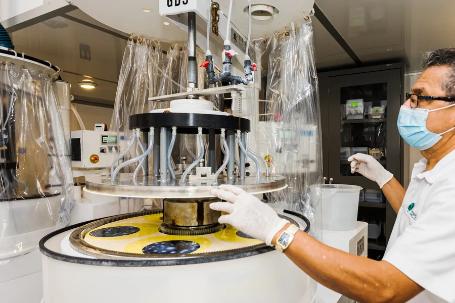
One difference rarely covered in comparison content is lifecycle cost. Because gallium arsenide is more expensive to produce than silicon, reclaiming process-monitor and production-reject wafers has become a standard cost-control step for companies running high volumes. Diameters from two to six inches can typically be reprocessed two to three times before the material is no longer viable, which significantly offsets the price gap with silicon over a production run.
Our GaAs and InP reclaim services page explains how that process works if you're trying to manage costs on a larger order.
In raw electron mobility, yes, but "faster" only matters if your circuit operates at frequencies where silicon's limitations actually show up. Below a few gigahertz, the difference rarely justifies the cost.
Its radiation tolerance and thermal stability outperform silicon in orbit, where temperature swings and particle radiation degrade solar cells over time.
Yes. Process-monitor and rejected wafers up to 150mm can be polished and reused multiple times, which is a meaningful cost lever given the material's higher base price.
No. Silicon still dominates consumer and industrial electronics. Gallium arsenide fills a narrower, higher-performance niche.
Choosing between silicon and gallium arsenide isn't a matter of picking the trendier material; it's about matching the substrate to the frequency, radiation, and thermal demands your design actually faces. Wafer World has spent over two decades helping engineers work through exactly this kind of specification, from prime GaAs wafer stock to reclaimed test-grade material for lower-budget runs.
If you're ready to talk through diameters, grades, or lead times for your next order, contact our team, and we will help you land on the right material the first time.




