Indium phosphide plays an important role in semiconductor technologies where high-frequency operation and photonic capabilities matter. As applications become more specialized, substrate selection also becomes more deliberate. For organizations considering InP reclaim wafers, quality is not simply a matter of whether a previously used substrate can be processed again.
Its physical condition, surface preparation, dimensions, cleanliness, and compatibility with the intended process all deserve attention before the material returns to a working environment.
InP is a III-V compound semiconductor with established roles in communications and high-frequency electronics. NIST research has examined InP monolithic microwave integrated circuits at frequencies reaching the terahertz range. In contrast, NASA research has investigated InP-based heterojunction bipolar transistors for high-frequency and high-power applications.
The material is also important to modern photonics. In 2026, the U.S. Department of Commerce’s CHIPS Program Office highlighted InP-based photonic devices as important for high-speed optical interconnects used to move data between processors, memory, and other systems in advanced data centers.
These applications help explain why substrate conditions deserve careful attention. A wafer intended for specialized development or fabrication should be evaluated in the context of what the next process will ask of it.
A reclaimed substrate has already undergone some form of prior use or processing. That history matters. Before reuse, it is useful to understand what materials, films, or residues may have been present and whether previous operations could have changed the substrate.
A wafer that appears acceptable under ordinary lighting may still carry surface species that interfere with later processing. NIST research on wet chemical cleaning of InP surfaces found that residues from plasma exposure can impede wafer processing. The study also illustrates an important point for reuse: surface preparation must address the chemistry present on the substrate, not simply its visible appearance.
For this reason, the suitability for reclamation should be considered process-specific. The objective is not merely to make a wafer look clean. It is to establish whether the resulting condition is appropriate for what comes next.
Surface finish and cleanliness are closely related, but they are not identical. Surface preparation may involve removing unwanted films or affected material, while cleaning focuses on unwanted chemical species or particles that remain on the substrate.
NIST notes that wet chemical cleaning is performed before many semiconductor processing operations, including epitaxial growth and deposition of metal or dielectric films. The purpose is to remove unwanted species residing on the wafer surface.
For reclaimed material, buyers may want to review factors such as:
No single item establishes quality by itself. The combination should fit the requirements of the intended process.
Reclaim processing may involve material removal. Whenever material is removed from a substrate, dimensions deserve renewed attention. A wafer that originally met one thickness specification should not automatically be assumed to retain that same value after additional surface processing.
Diameter, thickness, edge condition, and other dimensional characteristics can affect compatibility with equipment and handling systems. This becomes especially relevant when wafers are used in research tools or production equipment designed around defined substrate dimensions.
The practical question is not whether a reclaimed substrate perfectly matches its original condition. Instead, buyers should determine whether its current condition falls within the requirements of the new application.
That distinction makes accurate specifications useful. They allow engineers and purchasing teams to evaluate the wafer in use today rather than relying solely on its original description.
Terms such as “high-quality” can be useful shorthand, but semiconductor applications need more specific information. A substrate suitable for equipment testing may not automatically be appropriate for epitaxial growth, device fabrication, process development, or electrical characterization.
NIST research involving InGaAsP on InP has shown how specimen nonuniformity can influence characterization measurements. The work examined X-ray and photoluminescence measurements and found that nonuniformity could affect measurement results.
That example reinforces a broader purchasing principle. Quality should be connected to measurable requirements and intended use rather than treated as one universal grade.
Advanced semiconductor work does not always involve final device production. Laboratories also need substrates for process trials, equipment setup, handling studies, deposition development, cleaning experiments, and other controlled work.
Reclaimed substrates may be worth evaluating for selected uses when their specifications are appropriate. However, the fact that a wafer is reclaimed does not establish that it is suitable for every non-production task.
A more useful approach is to define the process first. What will happen to the substrate? Will it experience cleaning, deposition, thermal processing, characterization, or another operation? Which physical and electrical characteristics are important to that work?
Answering these questions gives buyers a practical basis for comparing available material with the requirements of an experiment or process-development program.
The growing relevance of InP to communications and advanced computing also underscores the need for careful substrate selection. The Department of Commerce notes that InP photonics supports high-speed data transmission in AI systems, telecommunications, and advanced networks. NIST has also studied high-frequency measurements involving InP devices and heterogeneous circuits containing InP chiplets.
None of this means reclaimed substrates can automatically be substituted into those device-production environments. Instead, it demonstrates why InP is a technically important material and why reuse decisions should be based on the requirements of a specific application.
A productive supplier conversation should go beyond diameter and quantity. Buyers can ask what specifications are available, what surface condition is provided, and whether the material has characteristics relevant to their intended process.
It is also useful to identify which requirements are mandatory and which are preferred. Doing so can make material evaluation clearer and reduce the risk of choosing a substrate based on assumptions.
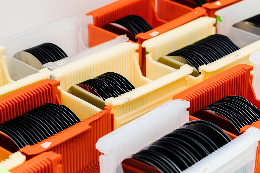
In general, reclaiming refers to preparing a previously used wafer for another suitable use. The exact processing performed can vary, so buyers should review the available specifications and condition of the actual material rather than assume every reclaimed substrate has undergone an identical sequence.
Not automatically. Suitability depends on the wafer’s current characteristics and the requirements of the intended process. Surface condition, dimensions, cleanliness, electrical characteristics, and other specifications may matter differently from one application to another.
Unwanted surface species can interfere with semiconductor processing. NIST research on InP cleaning specifically reports that certain plasma-generated oxide residues impede wafer processing. This is why cleanliness should be evaluated based on the next operation the substrate will undergo.
Yes, when thickness is relevant to the application. If reclaim preparation removes substrate material, buyers should rely on the wafer’s current specifications rather than assume its original dimensions remain unchanged.
Not necessarily, but their suitability for any advanced task must be established from the actual specifications and process requirements. Reclaimed material may be considered for research, process development, equipment-related work, or other applications when its characteristics meet the necessary criteria.
Choosing InP reclaim wafers starts with a clear understanding of the process they need to support, from dimensions and surface conditions to cleanliness and other application-specific requirements. Wafer World can help you review available material specifications and determine which options are worth considering for your research, testing, or semiconductor work.
Contact us to schedule a consultation or call to discuss your substrate requirements and plan your next project with better material information.




