.webp)
One of the many ways that wafers are processed includes wafer separation and surface refinement. In this process, a single crystal is turned to the desired diameter before bed light with one or two flats. Different wafer sizes are produced during this process, including flat wafers and ultra-flat wafers. If you want to learn more, here's how wafers are processed.

The crystal is sawn into thin discs, or wafers, using an annular saw with a diamond-splinter-filled cutting edge. The saw offers high accuracy while sawing smoothly. Due to the width of the blade, up to 20% of the crystal rod can be lost. However, wire saws, which allow multiple wafers to be cut from the staff at once, are used more frequently today.
As a result, a long wire is led through rotating rollers while wetting with silicon carbide grains and a carrier (glycol or oil) suspension. The silicon crystal is cut into single wafers after being drained into the wire grid. The wire has a typical thickness of 0.1-0.2 mm and moves counterclockwise at a speed of about ten m/s.
After cutting, the slices have a rough surface, and the crystal lattice has been damaged by mechanical stress. The wafers go through several steps in the process to finish the surface.
On a rotating steel disc, 50 microns (0.05 mm) of the wafer surface are removed using granular abrasives (for example, aluminum). The mechanical treatment again harms the surface even though the grain size is gradually reduced. After lapping, there is a 2-micron flatness.
The discs must not have any sharp edges in the subsequent processes because otherwise, the deposition of the layers could flake off. Therefore, a diamond cutter is used to round the silicon wafers' bevels.
Fifty microns are eliminated through a second wet etch process using a hydrofluoric, acetic, and nitric acid solution. The process is chemical, so the surface is not harmed. Defects in crystals are eliminated in the process.
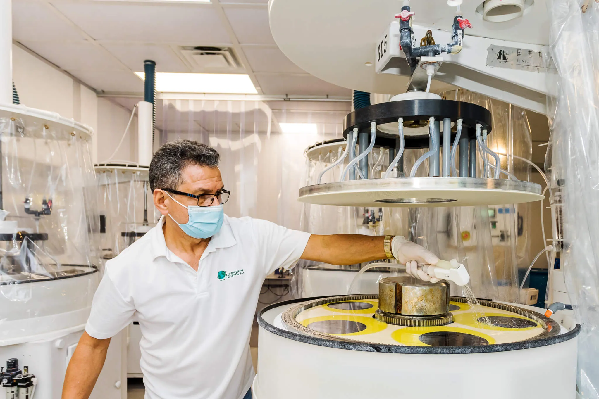
The process of surface refinement ends with this step. After polishing, the wafers have no more than a 3 nm bump. A solution of sodium hydroxide (NaOH), water, and silicon oxide grains is used to treat the wafers. The hydroxide removes machining marks left by the oxide grain, while the oxide removes an additional 5 microns from the surface.
At Wafer World, we can provide you with ultra-flat wafers and other related materials for your industry. Give us a call today to request a quote!


