Central Processing Units, or CPUs, are the brains of modern electronics. From smartphones to supercomputers, these chips power our digital world. But have you ever wondered how a CPU is made? This intricate manufacturing process involves several critical steps from an SI wafer to a fully functional microprocessor.
Although CPU operation may appear magical, it is the product of decades of astute engineering. As transistors, the fundamental building blocks of any microchip, shrink to microscopic scales, the manufacturing process becomes increasingly complex.
Some of the key stages of the CPU manufacturing process include:
A CPU's journey begins long before any physical material is present. It begins in the minds of engineers. Chip architects now specify the CPU's capabilities, including clock speeds, power consumption, number of cores, and features like integrated graphics or AI acceleration. This process involves:
1. Creating the instruction set
2. Defining the logic circuits
3. Simulating how the chip will perform under various conditions
After the design is complete, software tools convert it into a layout. This digital blueprint, a mask layout, acts as a map for each CPU layer.
The finalized design is then utilized to make a photomask, a high-precision glass plate with the circuit patterns on it. Every layer in the CPU design has a matching photomask.
These masks will subsequently be used to etch the chip's microscopic features onto the silicon wafer using photolithography.
A thin, round piece of extremely pure silicon, a Si wafer, is the central component of every CPU. Silicon is used due to its semiconductor properties, which allow it to conduct electricity under specific circumstances.
The process includes:
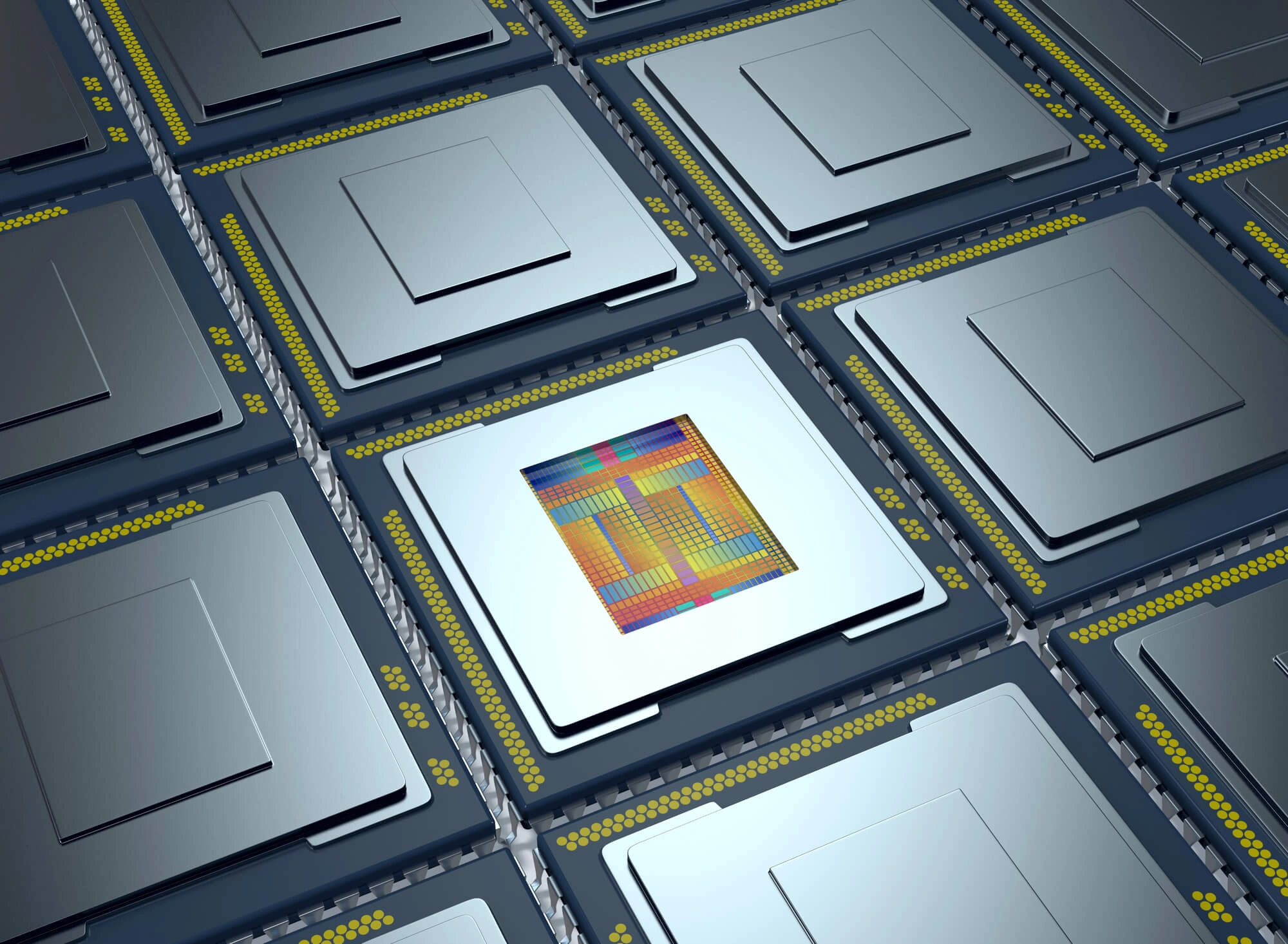
Each Si wafer can hold hundreds of individual CPU chips called dies.

Transistors are the building blocks of CPUs. Modern processors contain billions of transistors packed into an area smaller than a fingernail. These tiny switches are created by manufacturers layering and patterning materials onto the Si wafer using photolithography, ion implantation, and etching.
This step involves:
This multi-step process is repeated to build up the CPU layer by layer—often as many as 30–50 layers.
After the transistors are positioned, they must be connected to function as a unit. Metal interconnects, usually composed of aluminum or copper, are used for this.
These interconnects, which link millions or billions of transistors in intricate configurations, make up the CPU's wiring system. The metal layers are deposited and etched using sophisticated methods such as dual damascene.
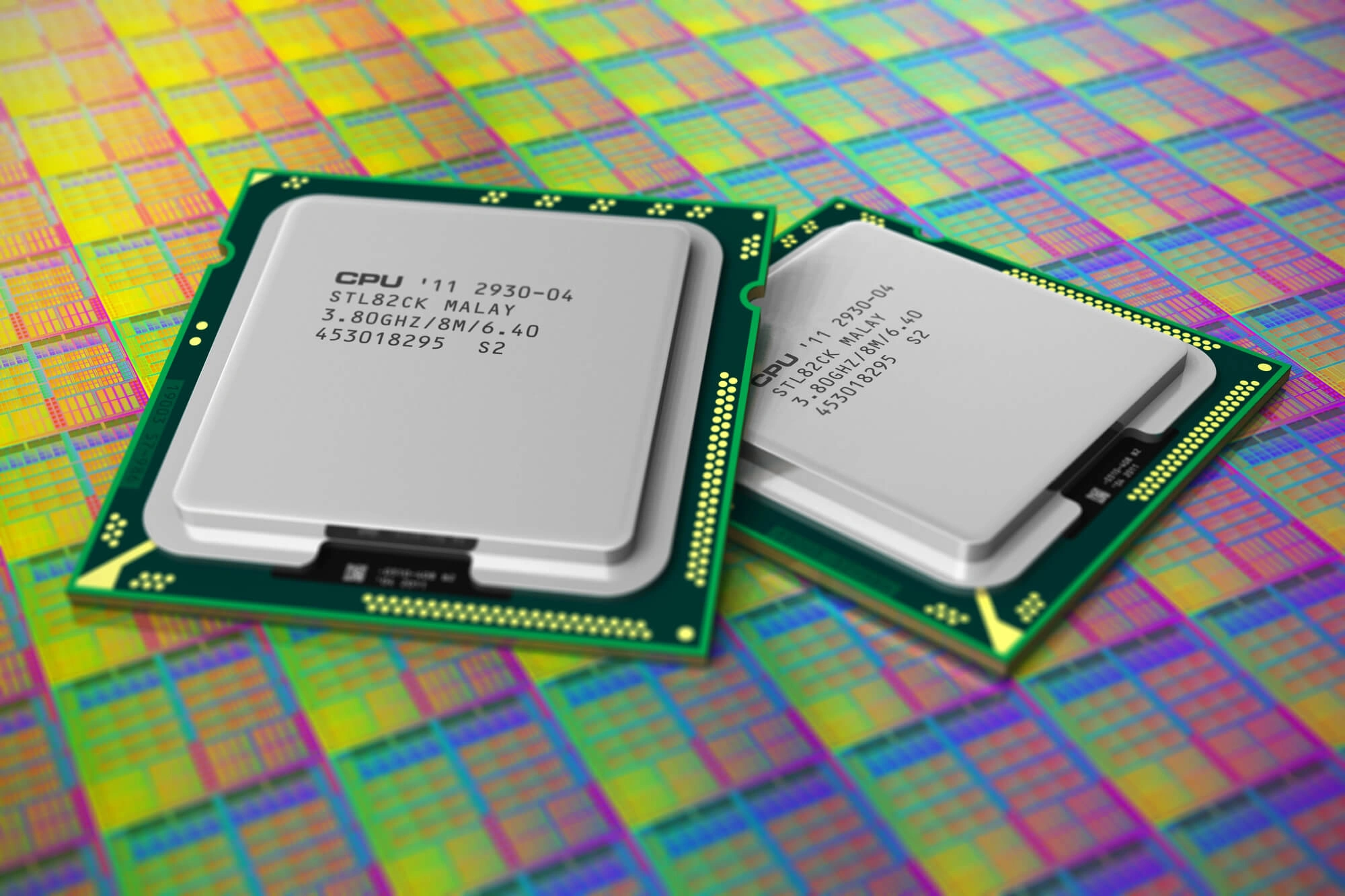
Once the circuits are finished, the Si wafer is cut into separate dies. Every chip on the wafer is put through a rigorous testing process because not all will work properly.
Following that, the functional CPU dies are packaged in a protective casing with electrical contacts (called pins or pads) and attached to cooling heat spreaders and thermal interface materials. They’re then retested to guarantee dependability and performance in practical settings.
The packaging must protect the delicate silicon so that it properly interfaces with other system components.
Some of the most advanced equipment on Earth is used to make a CPU. Leading manufacturers like Intel, TSMC, and Samsung invest billions in developing new fabrication technologies that push the limits of Moore’s Law. Some of the equipment used in producing a CPU include:
These tools operate in ultra-clean environments called clean rooms, where even a speck of dust can ruin a chip.
Photolithography is at the heart of CPU manufacturing. Without it, we couldn’t print the microscopic patterns needed for modern processors. As features get smaller, photolithography has evolved from deep ultraviolet (DUV) light to extreme ultraviolet (EUV), allowing even finer detail.
To continue advancing performance, chipmakers are turning to 3D integration. This involves stacking chips or components vertically, reducing latency and increasing bandwidth.
Examples include:
This approach offers better performance per watt and scalability for future processors.
You might think the hard part is over once the CPU die is complete—but packaging plays a crucial role in performance and longevity.
Modern packaging techniques include:
Proper packaging ensures the chip can operate safely and communicate efficiently with the motherboard and other components.

From raw Si wafers to powerful, intelligent microprocessors, the journey of a CPU is one of the most complex and impressive feats of modern engineering. Each CPU contains astonishing precision and innovation, with billions of transistors etched in atomic layers, all built on a slice of silicon smaller than a pancake.
Understanding how CPUs are made not only helps us appreciate the devices we use every day but also illuminates the future of computing. Would you like a silicon wafer for your project? Contact Wafer World today for more information!


