Every CPU begins with something surprisingly simple: sand. Silicon, derived from purified quartz, is the foundation of all modern processors. After being refined into ultrapure silicon, the material is melted and crystallized into large cylindrical ingots, which are then sliced into thin, mirror-smooth double side polish wafers, laying the groundwork for the most complex manufacturing process on the planet.
But, how does that process go in detail?
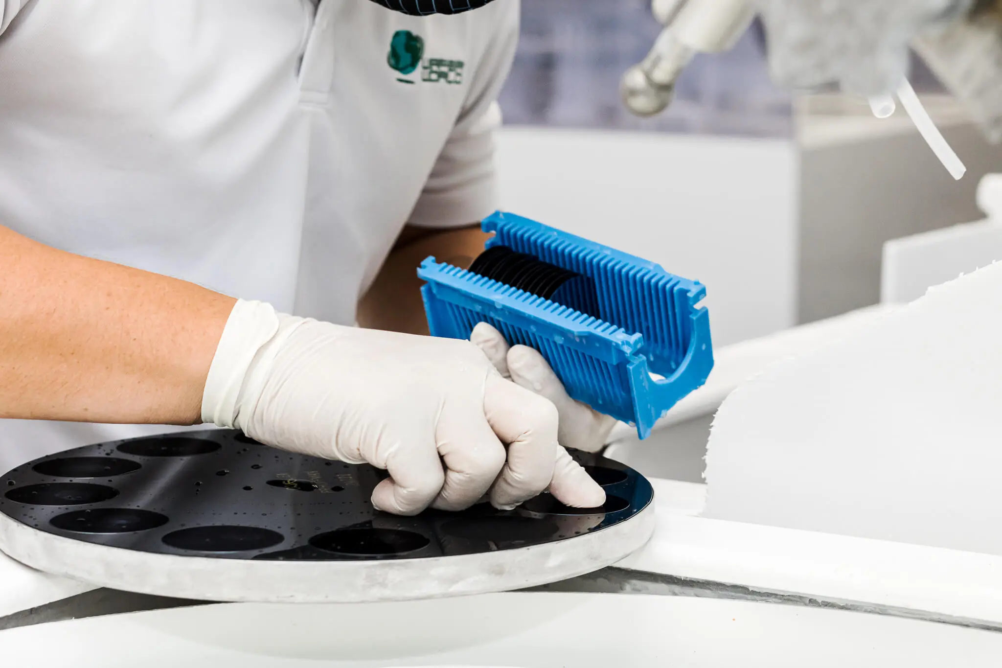
Wafers are the base upon which billions of microscopic transistors will be built.
For CPUs, double side polished wafers are used to ensure uniform thickness, minimal warp, and atomic-level smoothness on both surfaces. This perfection is essential—any surface variation could distort the photolithography patterns that define transistor features measured in nanometers.
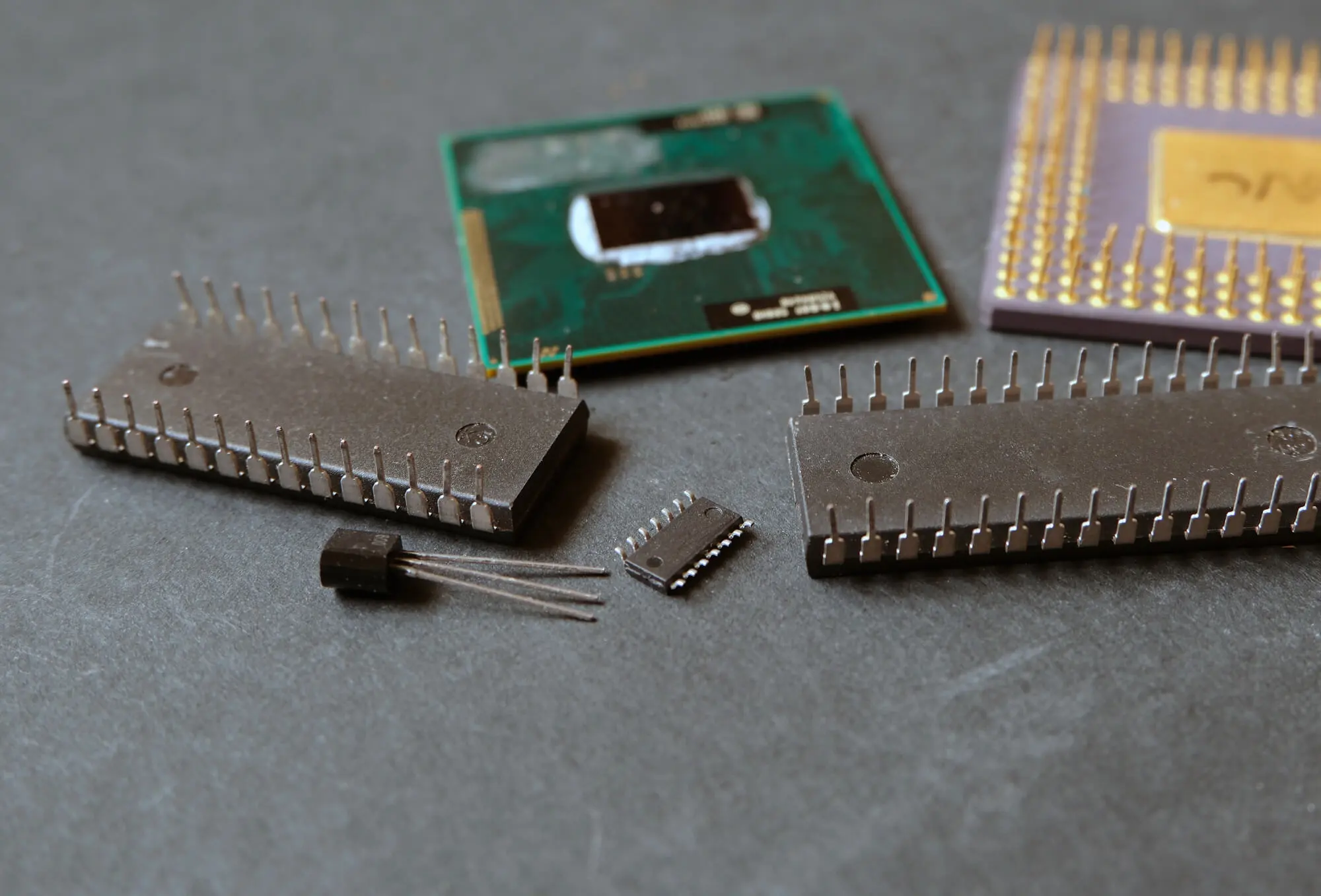
Before fabrication begins, chip architects design the CPU’s logic, that is, considering billions of interconnected transistors optimized for speed, power, and efficiency.
This design is converted into a set of photomasks, which serve as stencils for the light patterns used in the lithography process. Each mask layer represents a different part of the transistor structure or metal interconnect.
Using the photomasks, light is projected onto the wafer coated with photoresist, transferring the microscopic circuit patterns layer by layer. Through repeated etching, doping, and deposition, transistors are built into the silicon, one by one.
Once the transistors are finished, metal interconnects are deposited to connect them into functional circuits. Copper and other conductive materials are layered and patterned to create intricate three-dimensional wiring networks. The result is a functioning CPU core capable of performing billions of calculations per second.
Finally, following fabrication, the wafer is electrically tested to identify fully functional dies.
Each working die is separated from the wafer ("dicing") and packaged to protect the chip and connect it to the motherboard.
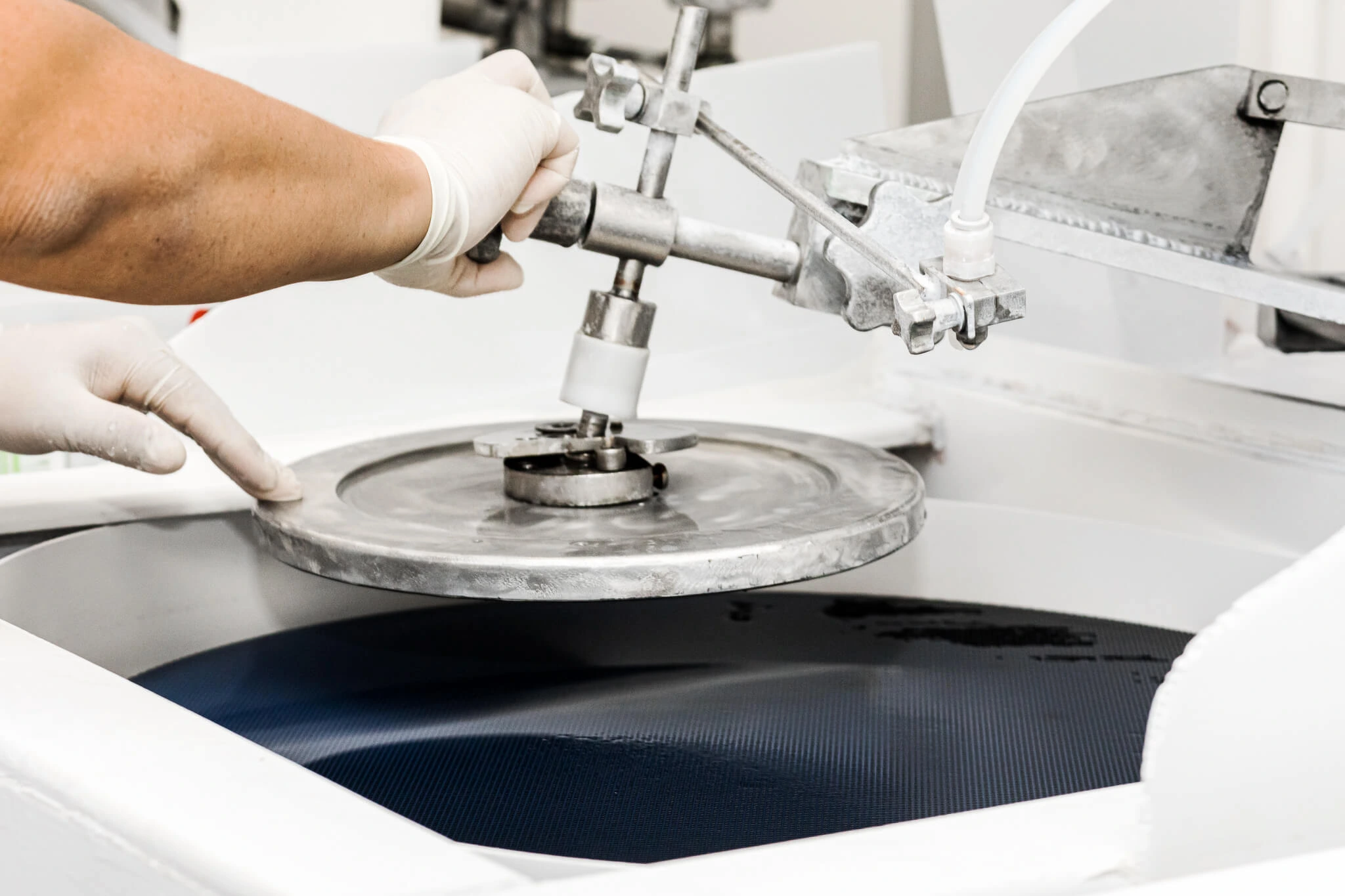
The process of making CPUs is a blend of physics, chemistry, and engineering artistry. From pure silicon to advanced 3D transistor architectures, every step relies on precision—and that precision begins with the wafer itself. The wafer’s double-sided polish ensures perfect focus and alignment for every layer across the wafer surface.
If you’d like to learn how our double-sided polish wafers can help you achieve superior yields and performance in your semiconductor manufacturing processes, contact Wafer World today!


