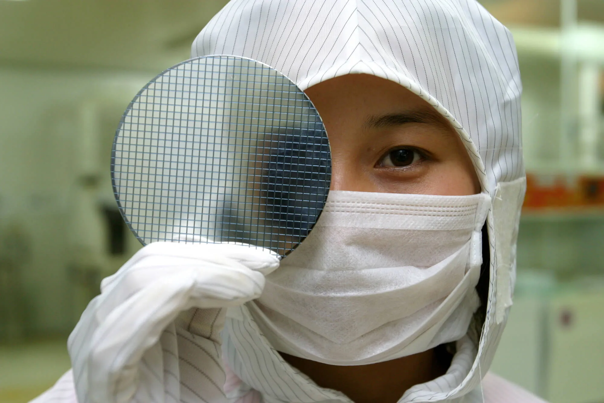
The quality of the silicon wafers is critical to the performance and reliability of these devices, making the manufacturing process a highly precise and complex operation. In this article, we will explore the silicon wafer processing and manufacturing, from raw material acquisition to final wafer characterization and inspection.
Silicon wafer processing refers to the manufacturing steps involved in producing high-quality silicon wafers for use in semiconductor devices such as microprocessors, memory chips, and sensors. The process involves converting raw materials such as silica sand into pure silicon.
The growth of silicon crystals using the Czochralski process, the slicing of the crystals into thin, flat discs, and the cleaning and preparation of the wafers for use in semiconductors devices. The quality of silicon wafers is critical to the performance and reliability of semiconductor devices, and manufacturers must use high-quality wafers to produce high-quality products.
The primary raw material used in silicon wafer manufacturing is silica sand, which is abundant in nature. However, not all sand is suitable for manufacturing high-quality silicon wafers. The sand must be high-purity, with low impurities, such as iron, aluminum, and other materials,to ensure that the resulting silicon wafers are high quality.
To obtain the necessary purity, the sand is washed and dried to remove any impurities affecting the silicon wafers' quality. It is then subjected to a high-temperature process to convert into pure silicon in large cylindrical ingots.
The most common method for growing silicon crystals for use in silicon wafer manufacturing is the Czochralski process. The process involves heating a germanium or silicon seed crystal and dipping it into molten silicon, gradually solidifying around it to form a cylindrical crystal. The crystal is rotated as it grows to ensure a uniform crystal structure and minimize impurities.
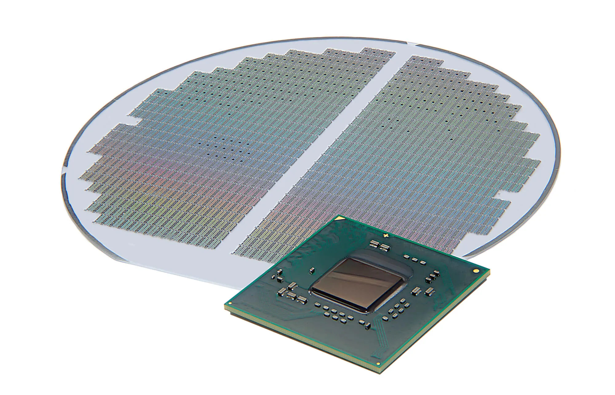
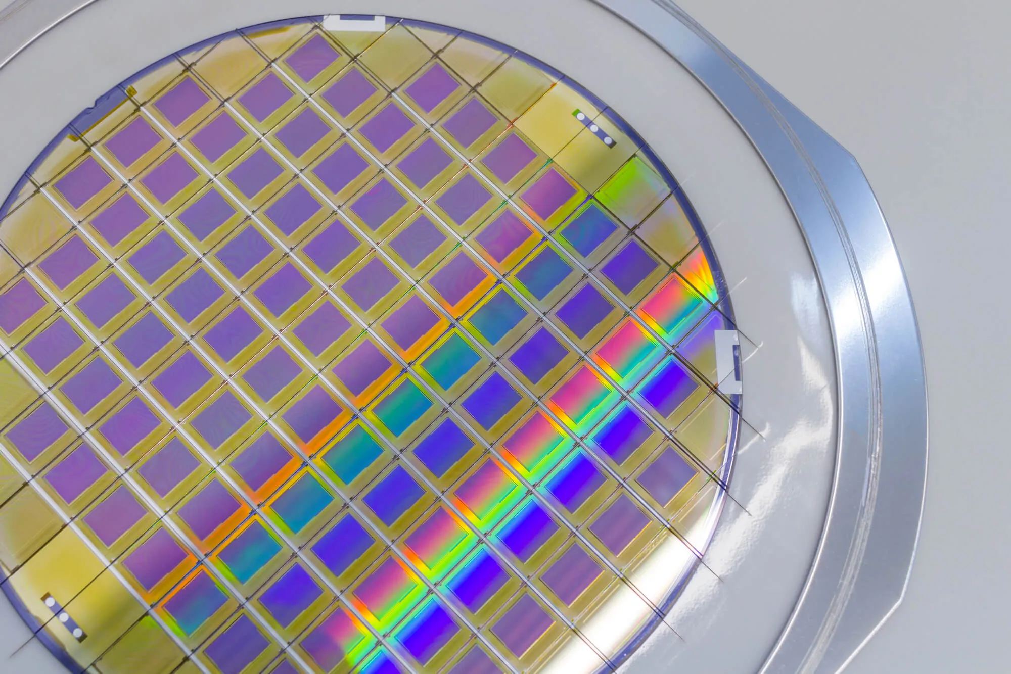
The crystal is doped with impurities, such as boron or phosphorus,to alter its electrical properties and make it suitable for semiconductor devices. The crystal is then sliced into thin, flat discs using a diamond saw, which are then polished to remove any surface defects and impurities.
The silicon wafers are subjected to chemical and mechanical cleaning processes to remove residual impurities and prepare the surface for further processing. The wafers are polished and ground to ensure that they are flat and have a uniform thickness, which is crucial for the performance of semiconductor devices.
The quality of the silicon wafers is critical to the performance and reliability of semiconductor devices. The wafers are measured for flatness and thickness to meet the required specifications. They are inspected for defects such as scratches, cracks, and contamination, affecting their performance in semiconductor devices. The wafers are also tested for their electrical properties, such as resistivity and carrier concentration, to ensure they are suitable for semiconductor devices.
Silicon wafers are essential in the semiconductor industry, serving as the building blocks for a wide range of electronic devices. Here are some of the key reasons why silicon wafers are so important:
Silicon wafers are made from high-purity silicon, which is critical for the performance and reliability of semiconductor devices. Even small amounts of impurities can significantly impact the electrical properties of the silicon and reduce the performance of the devices made from it. Therefore, the manufacturing process of silicon wafers involves several steps to ensure they are of the highest purity possible.
The electrical properties of silicon can be easily modified by adding impurities such as boron or phosphorus. This means that manufacturers can create silicon wafers with specific electrical properties to suit the needs of different types of semiconductor devices.
The manufacturing process of silicon wafers involves multiple steps that require a high degree of precision. For example, slicing the silicon crystals into thin, flat discs must be extremely accurate to ensure that the resulting wafers are uniformly thick and defects-free. This precision is crucial for the performance of semiconductor devices.
Silicon wafers can make a wide range of electronic devices, from simple diodes and transistors to complex microprocessors and memory chips. This versatility makes silicon wafers a valuable component in the semiconductor industry.
Advances in silicon wafer processing have played a significant role in developing the modern semiconductor industry. Researchers continually explore new methods for growing and processing silicon wafers to create more advanced and complex devices.
Silicon wafer processing has been a critical technology for the semiconductor industry for decades, but the field is still evolving rapidly. Here are some of the potential future directions for silicon wafer processing:
As semiconductor devices become more advanced and complex, the demand for high-quality silicon wafers will continue to grow. Researchers are exploring new methods for growing and processing silicon wafers to meet the increasing demand for high-performance semiconductor devices.
At Wafer World, our team can help you learn about silicon wafers and how they’re made. Get in touch with us today to get a free quote!


