
Electronic devices rely on semiconductor materials with stable electrical behavior, precise crystal structures, and minimal contamination. A float zone wafer is widely recognized for its exceptional purity because it is produced without direct contact between molten silicon and a crucible during crystal growth. This process helps reduce oxygen contamination and supports higher electrical consistency for advanced applications.
Because purity directly affects conductivity and defect levels, many manufacturers use float-zone materials in high-performance devices. These wafers are commonly selected for power electronics, detectors, RF components, and research applications where reliability is critical.

Impurities inside silicon can interfere with current flow, thermal performance, and overall device stability. High oxygen concentrations may introduce defects that affect long-term operation or reduce fabrication efficiency.
Float-zone processing minimizes these unwanted elements, allowing wafers to maintain cleaner crystal structures. This improved purity helps support stronger electrical resistance control and more predictable semiconductor performance.
Lower contamination levels can improve carrier lifetime, which is important in power devices and sensitive detection systems. Stable electrical behavior also helps manufacturers achieve more reliable fabrication results.
The reduced defect density found in float-zone materials supports applications that require precise signal handling or high-voltage operation. Industries working with radiation detectors, microwave devices, and specialized sensors often prioritize these material characteristics.
Consistent wafer quality helps semiconductor facilities maintain stable production conditions and reduce batch-to-batch variability. Uniform crystal structures also support smoother fabrication processes, especially in advanced electronic applications.
Organizations evaluating semiconductor materials often review purity, resistivity, and oxygen content together before selecting wafers for production or research environments.
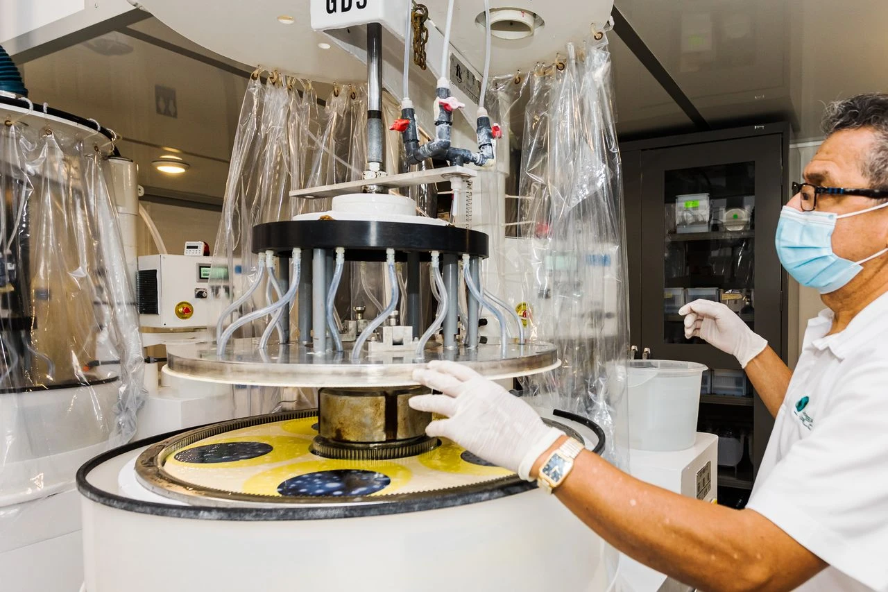
Understanding wafer purity can help manufacturers and researchers select materials that support stronger electrical stability and dependable long-term performance. If your team is evaluating float-zone wafer materials for semiconductor or industrial applications, carefully reviewing purity standards may help improve production consistency and device reliability. Wafer World provides silicon wafer solutions for technical and research environments. Contact us today to discuss your project requirements or connect with our team for additional information.




