In the ever-evolving world of semiconductor technology, precision and innovation are paramount. Float zone wafers have emerged as a critical component in the production of high-performance semiconductors. These specialized wafers offer unique advantages that are reshaping the landscape of electronics manufacturing. In this blog post, we will delve into the applications and advantages of float zone wafers, highlighting their significance in various industries.
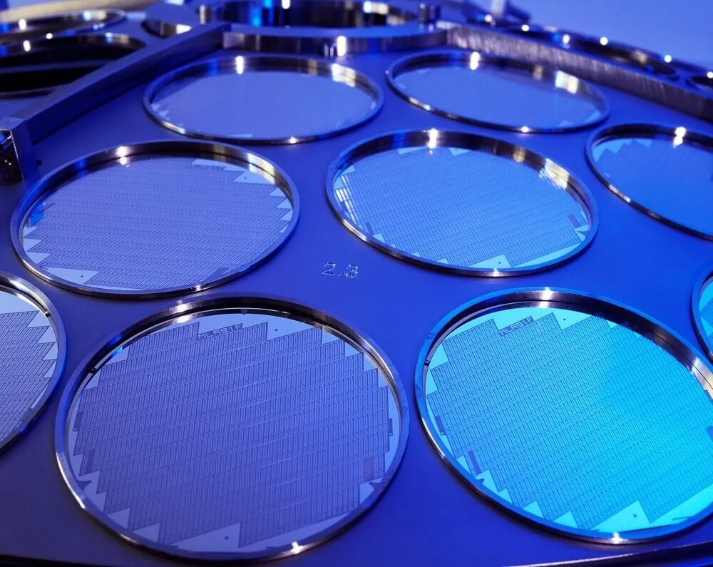
Float zone wafers are single-crystal silicon wafers that are manufactured using the Float Zone (FZ) method. This method involves carefully melting a silicon rod in a radio-frequency induction coil and then recrystallizing it into a single-crystal ingot. Unlike traditional Czochralski (CZ) wafers, which are grown from a seed crystal, float zone wafers are grown directly from a polycrystalline feedstock. This unique growth process imparts several distinct advantages to float zone wafers.
High-Efficiency Solar Cells: Float zone wafers are highly sought after in the solar industry. Their superior crystallographic quality and reduced impurity levels make them ideal for the production of high-efficiency photovoltaic cells. The increased light absorption and electron mobility of these wafers result in solar panels that can convert sunlight into electricity more efficiently.
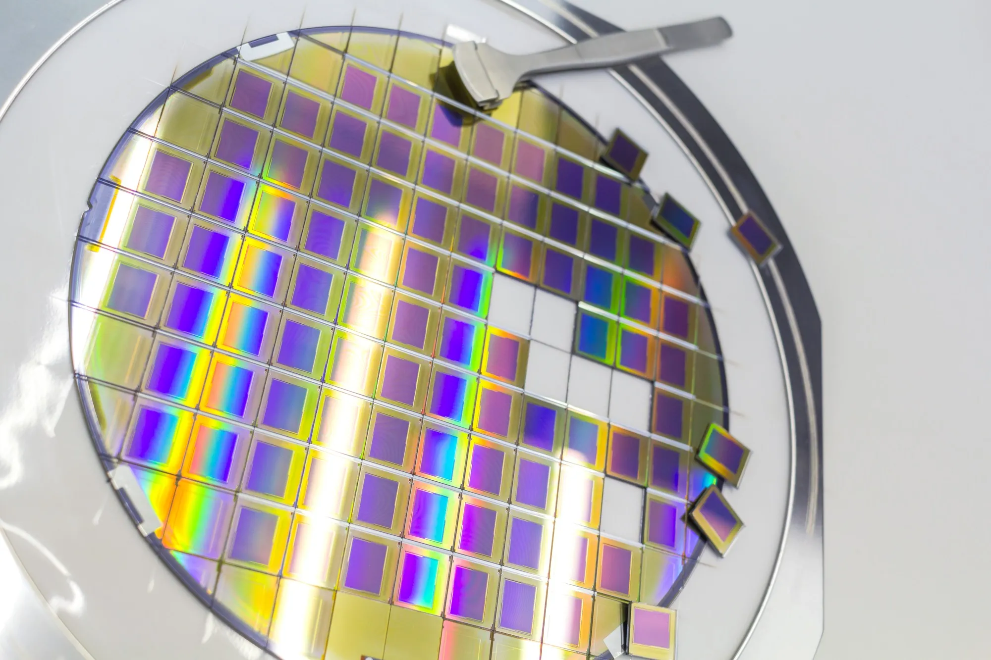
Float zone wafers are indispensable in the fabrication of cutting-edge electronic devices. These wafers are used to manufacture high-performance transistors, diodes, and integrated circuits. Their low defect density and exceptional purity enable the creation of smaller, faster, and more reliable electronic components.
In the field of high-energy physics, float zone wafers are crucial for constructing particle detectors. Their exceptional material properties, such as high resistivity and minimal radiation damage, ensure accurate and reliable detection of subatomic particles.
As quantum computing advances, the demand for high-purity substrates becomes increasingly critical. Float zone wafers are finding applications in the development of quantum devices, where the absence of defects and impurities is essential for maintaining quantum coherence.
Float zone wafers are renowned for their exceptionally high purity. The absence of impurities and defects in the crystal lattice results in improved electronic properties, making them ideal for applications demanding the utmost precision.
The float zone growth method significantly reduces dislocation density compared to CZ wafers. This reduction enhances the overall quality of semiconductor devices and extends their operational lifespan.
Float zone wafers exhibit superior electrical characteristics, including higher carrier mobility and reduced leakage current. This translates to faster and more energy-efficient electronic devices.
Float zone wafers can be customized to meet specific requirements. Their growth process allows for tailoring the material's electrical and mechanical properties to suit the needs of various applications.
In semiconductor manufacturing, metal contamination can have detrimental effects on device performance. Float zone wafers have a lower risk of metal contamination during the growth process, ensuring consistent and reliable results.
Float zone wafers exhibit excellent thermal stability, making them suitable for high-temperature applications. Their resistance to thermal stress and minimal warping ensure the reliability and longevity of devices in extreme operating conditions.
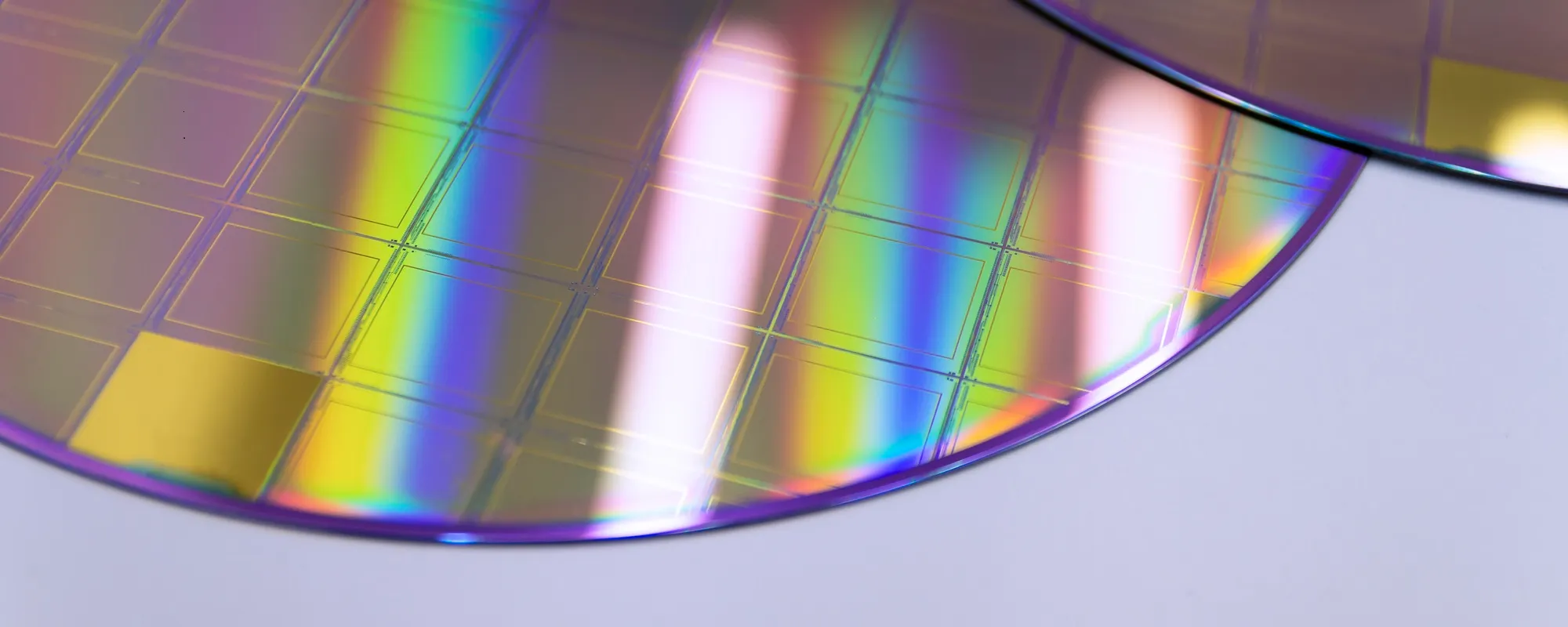
The float zone growth process results in wafers with smoother and more uniform surfaces. This property is crucial for applications where precise surface topography is required, such as in microelectromechanical systems (MEMS) and nanotechnology.
In aerospace and nuclear industries, where radiation exposure is a concern, float zone wafers excel. They have a higher tolerance for ionizing radiation, making them an ideal choice for manufacturing components used in space exploration and nuclear reactors.
Float zone wafers possess excellent mechanical properties, including higher fracture toughness and tensile strength. This characteristic is advantageous for applications that require robust and durable semiconductor substrates, such as power electronics and sensor devices.
The float-zone method stands out as an eco-conscious approach to silicon wafer production. Unlike other methods, such as the Czochralski (Cz) process, the float-zone method offers several environmental benefits:
In the float-zone process, silicon crystals are melted and drawn up from a molten pool, resulting in minimal material loss compared to the Cz method, which often generates a significant amount of wasted silicon.
Float-zone wafers require less energy for production because the method's unique characteristics allow for precise control of the heating process, reducing overall energy consumption.
Float-zone wafers generally require fewer chemical additives during production, further reducing their environmental impact compared to wafers produced using other techniques.
The float-zone method results in wafers with fewer impurities, which can lead to more efficient semiconductor devices and less electronic waste over time.
Wafers manufactured using the float-zone method are often of higher quality, leading to more durable and longer-lasting electronic components, ultimately reducing the need for frequent replacements.
Another aspect of the environmental impact of float-zone wafers is their potential for recycling and repurposing. As the technology industry strives for sustainability, reusing silicon wafers can significantly reduce waste and lower the demand for new wafer production. Float-zone wafers, with their high purity and quality, are prime candidates for recycling, extending their life cycle and minimizing environmental harm.
Innovation plays a pivotal role in minimizing the environmental impact of semiconductor manufacturing. As the demand for advanced technology continues to grow, the industry must explore new methods and materials that further reduce waste, energy consumption, and chemical usage. Float-zone wafers exemplify how innovative techniques can lead to more sustainable practices within the semiconductor industry.

Float zone wafers have ushered in a new era of precision, performance, and eco-friendliness in the semiconductor industry. Their remarkable purity, reduced defect density, and customized properties have made them indispensable in applications ranging from solar cells to quantum computing.
As technology continues to advance, the demand for float zone wafers is expected to grow, further solidifying their place as a cornerstone of modern electronics and materials science. These wafers are not just components; they are catalysts for innovation and progress in the digital age.
With Wafer World, you have access to the best wafer production chain in the market! Call now to order!


