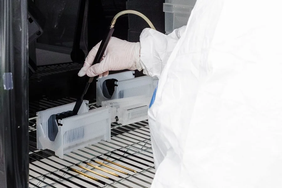
The evolution of float zone wafer production reflects decades of innovation driven by the growing demand for cleaner, more reliable semiconductor materials. From its early development to today's highly refined manufacturing techniques, float-zone wafer technology has continually improved to meet the needs of industries that rely on exceptional electrical performance, low impurity levels, and consistent material quality.
Understanding this progress offers valuable insight into why this manufacturing process remains an important choice for specialized applications.
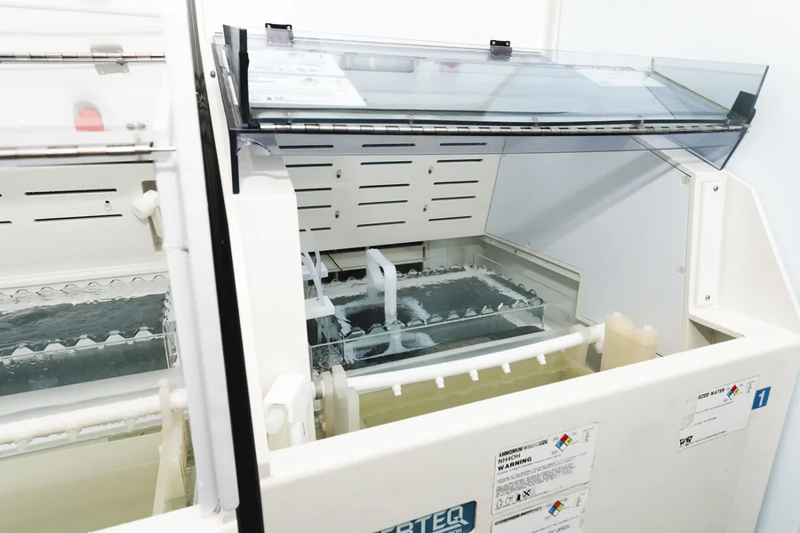
As semiconductor technology advanced, manufacturers quickly recognized the limitations of traditional crystal growth methods for certain applications. Devices requiring superior electrical characteristics needed silicon with significantly fewer impurities and defects. This challenge encouraged researchers to develop alternative production techniques that minimize contamination while producing highly uniform crystals.
The float zone process emerged as an effective solution because it avoided direct contact with a crucible during crystal growth. This greatly reduced unwanted impurities, allowing manufacturers to produce silicon suitable for demanding applications such as power electronics, radiation detectors, and research equipment.
Today's manufacturing environment combines decades of engineering experience with advanced automation and precision control. Every stage of production is carefully monitored to achieve consistent crystal quality while maintaining strict process standards.
Several developments have contributed to these improvements:
These advancements have helped manufacturers meet increasingly complex performance requirements across multiple industries.
As electronics become increasingly sophisticated, manufacturers face growing expectations for materials that deliver dependable, long-term performance. High-purity silicon remains essential for applications involving high voltages, demanding operating conditions, and specialized research.
Ongoing investments in manufacturing technology continue to improve efficiency, quality control, and production consistency. Future innovations may further optimize crystal growth techniques while supporting the development of next-generation semiconductor devices used in renewable energy, communications, medical technology, and industrial systems.
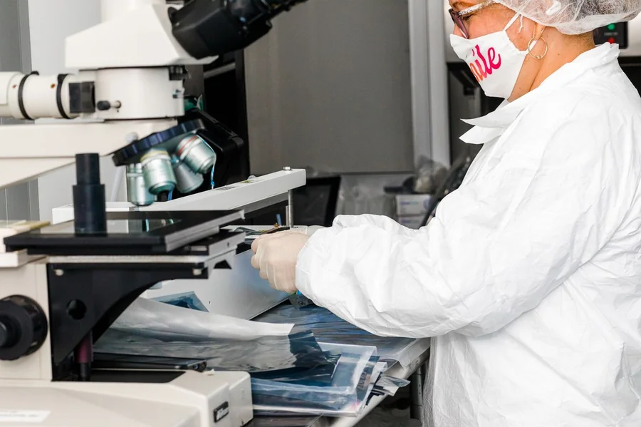
Choosing the right semiconductor material begins with understanding how manufacturing quality affects performance. Whether supporting research, advanced electronics, or specialized industrial applications, selecting materials produced through carefully controlled processes can yield more consistent and reliable results over the long term.
At Wafer World, we are committed to providing high-quality semiconductor materials while helping customers better understand the technologies that support their projects. If you would like to learn more about float zone wafer solutions or discuss your application requirements, contact us today to schedule a consultation with our team.




