As demand for faster communication, higher data capacity, and more advanced sensing technologies continues to grow, InP wafers have become an important material supporting the evolution of photonic devices. Industries ranging from telecommunications to healthcare increasingly rely on photonics to move, process, and detect information using light instead of electrical signals alone. This shift is helping create systems that are faster, more efficient, and better able to handle the growing demands of a connected world.
Photonics has become one of the most significant technological fields because it enables the transmission and manipulation of light for countless applications. From fiber-optic networks and data centers to autonomous vehicles and medical equipment, photonic technologies are helping drive innovation across multiple sectors. Behind many of these advances are specialized semiconductor materials that enable optical performance.
Photonics focuses on generating, controlling, transmitting, and detecting light. Similar to how electronics uses electrons to process information, photonics uses photons. The result is often greater speed, lower power consumption, and improved performance in applications that require rapid data movement.
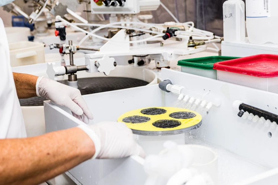
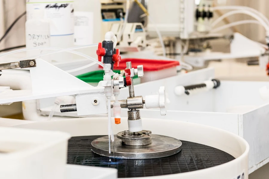
The effectiveness of photonic devices depends heavily on the semiconductor materials used during manufacturing. Different materials possess unique electrical and optical properties that influence how efficiently they can emit, detect, or guide light.
Material selection affects:
Choosing the right substrate material can significantly impact the performance of lasers, detectors, modulators, and integrated photonic circuits.
Indium phosphide has attracted widespread attention for its ability to operate efficiently at wavelengths commonly used in optical communications. These wavelengths align well with existing fiber-optic infrastructure, making the material highly valuable for modern networking systems.
Several characteristics contribute to its importance:
High electron mobility allows devices to operate at elevated frequencies while maintaining efficient performance. This capability supports high-speed communications and advanced signal processing applications.
Unlike some semiconductor materials, indium phosphide features a direct bandgap. This characteristic enables efficient light emission, making it well-suited for laser-based technologies and optical transmitters.
The material demonstrates excellent optical properties across wavelength ranges widely used in telecommunications, sensing, and photonic integration. These properties help improve overall device efficiency.
Modern photonic systems often require multiple functions to exist within a compact footprint. The material's characteristics support the integration of lasers, detectors, modulators, and other components on a single platform.
As photonic technologies continue expanding, several industries increasingly depend on high-performance semiconductor substrates.
Global internet traffic continues to rise as cloud computing, video streaming, artificial intelligence, and connected devices generate unprecedented data volumes. Fiber-optic communication systems rely on advanced photonic components to maintain speed and reliability.
Optical transmitters, receivers, and amplifiers help move information across long distances while minimizing signal loss. These systems form the backbone of modern communications infrastructure.
Data centers require rapid movement of enormous amounts of information between servers and storage systems. Optical interconnects help overcome bandwidth limitations associated with traditional electrical connections.
Photonic technologies improve data transmission rates while reducing energy consumption, making them increasingly valuable in large-scale computing environments.
Photonic sensors are becoming essential across industries that require precise measurement and monitoring capabilities.
Examples include:
Many sensing platforms benefit from highly responsive optical components that detect subtle changes in light signals.
Medical imaging and diagnostic systems increasingly incorporate photonic technologies. Optical tools can provide highly detailed information while supporting minimally invasive procedures and advanced analytical techniques.
As healthcare technology evolves, demand for reliable photonic components is expected to continue growing.

Several trends are accelerating investment in photonics worldwide.
Artificial intelligence infrastructure requires faster data movement between computing resources. Next-generation wireless networks demand higher capacity and improved performance. Autonomous systems depend on sophisticated sensing technologies to accurately interpret their surroundings.
At the same time, researchers continue developing photonic integrated circuits that combine multiple optical functions onto increasingly compact platforms. This approach can reduce system complexity while improving efficiency and scalability.
Governments, research institutions, and technology companies are investing heavily in photonics because of its potential to support future applications in communication, computing, healthcare, and sensing.
While photonics offers substantial advantages, manufacturers continue working to address challenges related to device complexity, production scalability, and integration with existing technologies.
Ongoing research focuses on improving manufacturing processes, increasing yield, and enhancing overall device performance. Advances in fabrication techniques are helping make photonic technologies more accessible across a broader range of applications.
The opportunities remain significant. As industries seek faster communications, more capable sensors, and energy-efficient computing solutions, photonics is positioned to play an increasingly important role in technological development.
Its optical and electronic properties support efficient light generation, detection, and signal processing across applications such as telecommunications, sensing, and integrated photonic devices.
The telecommunications, cloud computing, healthcare, aerospace, industrial automation, environmental monitoring, and automotive sectors all use photonic systems to improve performance and efficiency.
Electronics primarily use electrons to transmit and process information, while photonics uses photons. This often enables faster data transfer and improved bandwidth capabilities.
They help move large volumes of data at high speeds while reducing energy consumption and supporting growing computing demands.

As photonic technologies continue transforming communications, sensing, healthcare, and computing, understanding the capabilities of InP wafers can help organizations make informed decisions about future device development and performance goals. If you would like to explore material options, technical considerations, or application requirements, contact Wafer World to schedule a consultation and discuss solutions that support your photonic innovation objectives.


