
The InP wafer has become a cornerstone material in advanced semiconductor engineering, enabling faster, more efficient electronic and photonic systems. As industries demand higher speeds and better signal integrity, indium phosphide continues to stand out due to its unique physical and electronic properties.
Indium phosphide is a III-V compound semiconductor known for its high electron mobility and direct bandgap. These characteristics make it especially effective for high-frequency and optoelectronic applications. Unlike silicon, which dominates general electronics, indium phosphide excels in environments where speed and optical efficiency are critical.
One of its defining features is its ability to operate efficiently at high frequencies, making it ideal for radio-frequency applications. It also performs exceptionally well in optical communication systems due to its compatibility with fiber optic wavelengths. These properties allow engineers to design devices that transmit data faster and with less signal loss.
Thermal stability is another advantage. While not as robust as silicon in some mechanical aspects, indium phosphide maintains consistent performance under demanding electrical conditions. This reliability is essential in telecommunications infrastructure and aerospace systems.
The production of indium phosphide wafers involves precise crystal growth techniques, such as liquid-encapsulated Czochralski methods. These processes ensure uniformity in crystal structure, which directly impacts device performance.
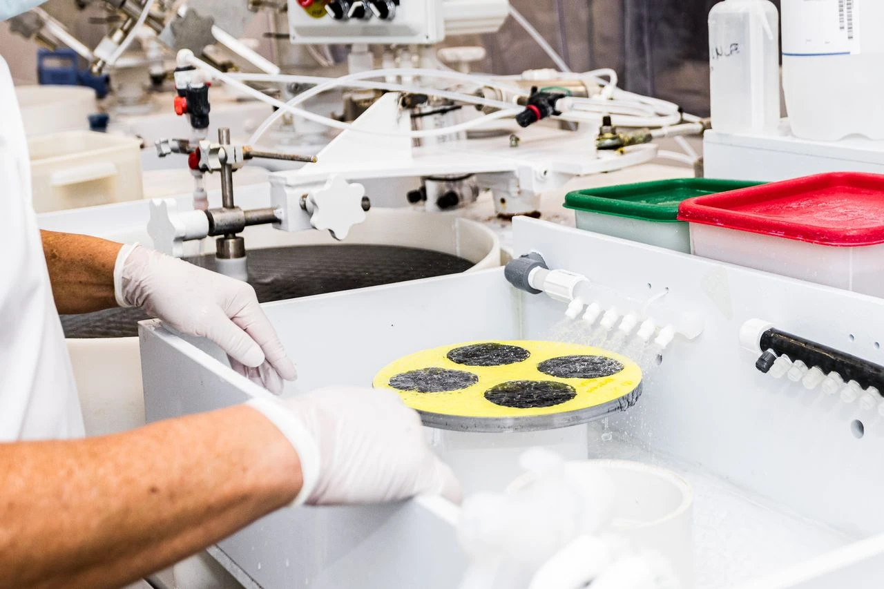
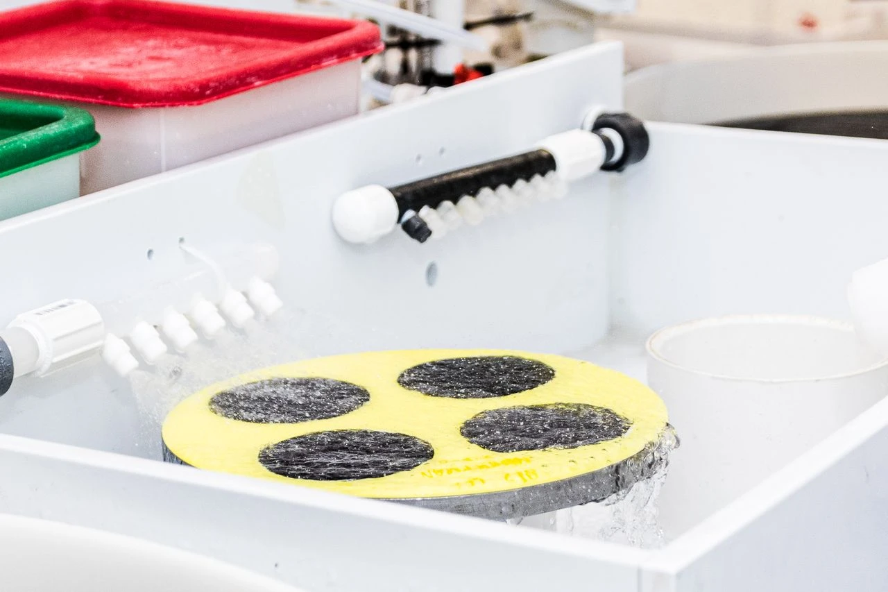
Surface quality is critical. Even minor imperfections can affect the efficiency of high-frequency or optical devices. As a result, polishing and cleaning processes are carefully controlled to achieve atomically smooth surfaces. This level of precision supports the fabrication of lasers, photodetectors, and integrated circuits.
Doping is another important aspect. By introducing specific impurities, manufacturers can tailor electrical properties to meet application requirements. This flexibility allows indium phosphide to be used across a wide range of technologies, from research labs to commercial systems.
Advancements in wafer reclaim and recycling have also improved sustainability. Reclaim processes restore used wafers to a near-original condition, reducing waste and lowering production costs without compromising quality.
Indium phosphide plays a critical role in modern communication networks. Its direct bandgap enables efficient light emission, which is essential for laser diodes used in fiber optic systems. These lasers transmit data over long distances with minimal loss, forming the backbone of global internet infrastructure.
Photodetectors made from indium phosphide are equally important. They convert optical signals back into electrical signals with high sensitivity and speed. This capability ensures reliable data transmission even in high-demand environments.
With the rise of 5G and future communication technologies, the demand for faster signal processing continues to grow. Indium phosphide enables components that operate at higher frequencies than traditional materials.
In radio frequency and microwave applications, indium phosphide offers unmatched performance. Its high electron velocity allows transistors to switch faster, making it ideal for amplifiers and high-speed integrated circuits.
These capabilities are particularly valuable in satellite communications and radar systems. Devices built on indium phosphide wafers can handle complex signals with precision, ensuring accurate data transmission and reception.
Another advantage is reduced noise. Low noise levels are essential in sensitive electronic systems, especially in defense and scientific instrumentation. Indium phosphide helps maintain signal clarity, even in challenging conditions.

Photonics is one of the fastest-growing fields benefiting from indium phosphide technology. From laser systems to optical sensors, this material enables innovations that go beyond traditional electronics.
In healthcare, indium phosphide-based devices are used in imaging and diagnostic equipment. Their ability to interact efficiently with light allows for more accurate detection and analysis.
Environmental monitoring is another area of application. Sensors built on indium phosphide platforms can detect gases and pollutants with high precision, supporting efforts to maintain air quality and safety.
Quantum computing and advanced research are also exploring the potential of indium phosphide. Its optical properties make it a candidate for developing quantum-level components, opening new possibilities in computing and data security.
Despite its advantages, working with indium phosphide presents challenges. The material is more brittle than silicon, requiring careful handling during processing. Manufacturing costs are also higher due to the complexity of crystal growth and wafer preparation.
However, ongoing research continues to address these limitations. Improved fabrication techniques and automation are helping reduce costs and increase scalability. As demand grows, economies of scale are expected to make indium phosphide more accessible.
Industry forecasts suggest steady growth in applications driven by telecommunications, automotive sensing, and advanced computing. As technologies evolve, the role of indium phosphide will likely expand further.
The semiconductor industry is constantly evolving, with new materials being explored alongside established ones. Indium phosphide remains a strong contender due to its proven performance in high-speed and optical applications.
Integration with other materials is one emerging trend. Hybrid systems that combine indium phosphide with silicon or other semiconductors aim to balance cost and performance. These approaches could lead to more versatile and efficient devices.
Another trend is miniaturization. As devices become smaller, the need for materials that maintain performance at reduced scales becomes critical. Indium phosphide meets this demand with its high efficiency and reliability.
Sustainability is also shaping the future. Recycling and reclaim processes are gaining importance as industries seek to minimize environmental impact. Indium phosphide wafer reclaim supports these goals by extending the life cycles of materials.
Choosing the right InP wafer solution requires a balance of quality, performance, and application-specific expertise. Whether you are developing high-frequency devices or advanced photonic systems, working with a knowledgeable partner can make a significant difference. At Wafer World, we support engineers and researchers with reliable wafer solutions tailored to evolving industry needs. Connect with us today to explore how we can assist with your next project and help bring your innovations to life.


