Most if not all of the modern technology we rely on is dependent on semiconductors. These components facilitate the transfer of electricity between the circuits that make your computer, phone, and appliances work. So, even as technology keeps changing, semiconductors will be needed for years to come, but not without some changes. The demand for faster and more advanced systems means that the semiconductor industry will have to adapt and utilize materials better suited for these demands. Furthermore, InP wafers are one of the best examples of this change as their specifications are well-suited for the faster devices that lie ahead. Let’s take a closer look at InP wafers and how they will help us move forward.

Semiconductors are materials that can conduct electricity at a rate somewhere between conductors and insulators. These can be made out of a single element or compound.
We can divide semiconductors into two categories – intrinsic and binary. Intrinsic semiconductors tend to be single elements with conducting qualities on their own that do not necessarily require doping. Binary semiconductors are compounds, meaning they are made out of two or more materials or elements.
Simply, most modern technology like computers and smartphones work by sending tiny electrical signals back and forth through circuits. These signals turn tiny switches on and off in specific patterns, resulting in a particular function. If we were to use insulators for the process, the currents would not get to where they need to be. On the contrary, if we were to use conductors, there would be no way of controlling the amount of electricity that gets through. This would result in burnouts and short circuits. Semiconductors make it possible to regulate these currents. They essentially work like tiny dams or doors, opening and closing the floodgates as needed.
There are several semiconductor materials. The most common are:
When each is used depends on the applications and the particular qualities of the material. For example, silicon is the most widely used because it can be implemented effectively in many applications, and it’s easy to fabricate. On the other hand, silicon carbide can withstand high temperatures, so it’s used in power devices that operate e heavy machinery.

InP stands for Indium phosphide, which is a binary semiconductor made out of indium and phosphorous. When white phosphorus and indium iodide are combined in high-pressure chambers with temperatures exceeding 400°C, they create a reaction that forms InP.
We talked about how the different materials we choose for semiconductors depend on their special attributes. Indium phosphide offers a faster electron velocity, which means that electron particles can travel between circuits faster. InP wafers also provide other excellent capabilities like:
InP semiconductors lose heat at a lower rate than other semiconductors, making them perfect for applications that utilize heat transfer.
Indium phosphide’s resistance to radiation means it can be used in extremely demanding settings like space.
Even the best semiconductors have a threshold at which they begin to lose some of the power they transfer. InP wafers have a much higher threshold, making them perfect for uses that require high-power transfers for prolonged periods of time.
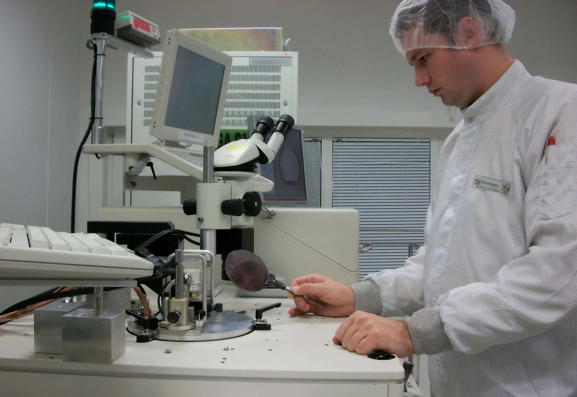
The process for making InP wafers is very similar to how other semiconductor wafers are made. The major difference comes in the creation of the compound. While intrinsic semiconductors like silicon need to be extracted and isolated from their natural source, binary semiconductors like indium phosphide first need to be turned into the compound from their respective elements. After the point, the progression is fairly standardized. Once ingots are made, they need to be sliced into the respective wafer shape and size. Then, they are polished and smoothed to create a surface primed for conductivity. The next step after the slice and polish is cleaning. This is important because all outside particulates that could compromise the intended conductivity need to be removed; otherwise, the semiconductor will not work how it’s supposed to. Finally, InP wafers are tested by being exposed to similar conditions to those they will experience in real-world applications. This includes high-temperature and voltage tests. Those that make it past this stage go on to be in an integrated circuit; those that do not are often reclaimed or recycled.
We all know that technology is moving at a breakneck pace. Our devices are getting faster and smarter, and so are networks. One of the most drastic demonstrations of this increased speed is the power of 5G technology and how much boosting information transfers. To keep up with these advancements, new technology requires semiconductors with stronger capabilities. This is where InP wafers come in. The superior electron velocity, thermal conductivity, and voltage breakdown resistance make this compound the leading choice to meet the rapidly evolving industry's demands. What’s more, InP wafers have a bright future beyond terrestrial applications. This new and faster technology is also going to be used in space. More private companies like SpaceX, Virgin, and Boeing are pushing the boundaries of what we once thought possible and planned on making more visits to the great void in the coming years. With its faster transfer capabilities and radiation resistance, InP will be at the front and center of the new space age.

The future is bright for technology, and Wafer World is excited to play a small part in making it possible. Therefore, knowing that our high-quality semiconductors will be the lifeblood of much of the next generation of electronics brings us great pride in what we do. If you want to learn more about semiconductors or are interested in our excellent products, get in touch today!


