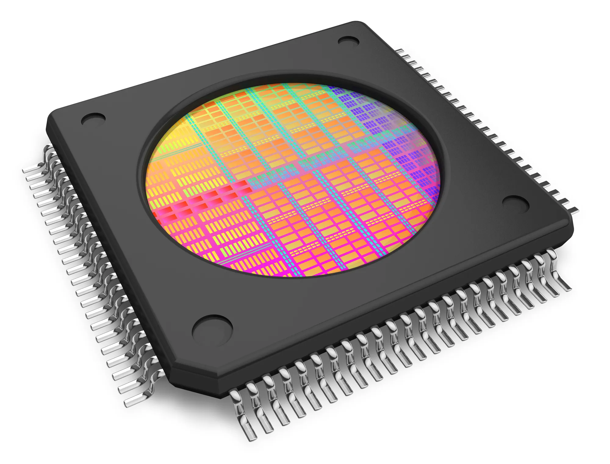
InP stands for Indium Phosphide. InP has a similar crystal structure to GaAs and other III-V semiconductors. Before an InP Wafer is produced, it goes through a series of multi-staged processes to ensure its quality. InP wafer is commonly used in high-frequency and high-power electronics. If you’re interested in InP wafers, here are the applications of InP wafers:
InP is known to possess a quality of superior electron velocity which makes it perfect for optoelectronic devices, rapid transistor, and resonance tunneling diodes.
Several material systems are now being utilized in the photonics market currently. Some of these silicon-hybrids include:
Before this new variation in the material system, the market was relatively small. This was due to how exclusive silicon was at the time. It was considered to be too expensive and laborious to work with. Because of this, scientists and engineers looked for a way to produce laser integrated circuits with a lower cost and higher functionality, thus creating hybrid silicon lasers.
Its most common medical field application is the optoelectronic devices because of the wide area of the wafer that can be used in the process. Not only are these wafers used to control devices for surgery, but also the monitoring of vital signs as well.
InP wafers possess the ability of higher electron mobility and saturation velocity. Because of this, InP wafers are suitable in the production of optical fiber transmission windows which are found in lasers and photodetectors.
InP has the capability to perform efficiently at a higher peak-to-valley ratio from larger thermal conductivity. InP is also able to produce optical fibers with minimal loss and diffusion.

Because of InP wafer’s superior quality, it is now considered to be the third most significant semiconductor in the world. Its various applications in advanced technology show that InP wafers have an even greater potential for more breakthroughs. Get quality InP wafer for your business and project needs at Wafer World. We are proud to be serving our clients with excellent wafers and exceptional customer service for more than 20 years. Be a part of our family! Call us today for any inquiry or purchase a wafer online!


