
Roughly 90% of the world's silicon wafers come from just five companies, according to the National Institute of Standards and Technology; that concentration is exactly why the CHIPS Act now funds new domestic wafer plants in Texas and Missouri. Most engineers never think about that supply chain until a shipment is delayed or a batch fails inspection. By then, it's too late to ask the right questions.
Understanding what actually happens between raw silicon and a finished wafer, a process Wafer World has refined since 1997, is what separates buyers who get burned from buyers who don't.
Silicon itself is not rare; as we cover on our page about silicon wafers, it's one of the most abundant elements on Earth, found in ordinary sand, quartz, and glass. What's rare is the equipment, expertise, and capital required to turn that raw material into semiconductor-grade crystal with defect densities low enough for modern chips. That barrier to entry is why the global market has remained concentrated for decades, and it's also why supply disruptions ripple so quickly through the electronics industry.
When you're vetting silicon wafer manufacturers, this concentration matters more than most buyers realize, because it directly affects lead times, pricing stability, and how much leverage you have if something goes wrong with an order.
The process starts with metallurgical-grade silicon, refined to semiconductor-grade purity, with roughly one impurity per billion atoms. That purified silicon is melted in a quartz crucible and then grown into a single-crystal ingot using the Czochralski method, which involves lowering a rotating seed crystal into the molten silicon and slowly pulling it upward. Researchers in a study published in the National Institutes of Health's PubMed Central archive have documented that even small changes in crucible rotation speed alter oxygen concentration in the finished crystal, underscoring how sensitive this stage really is.
A few rotations per minute in either direction can shift the electrical properties of every wafer sliced from that ingot.
Before or during the melt, manufacturers add controlled amounts of boron or phosphorus to set the wafer's electrical conductivity type and resistivity. Get the dopant ratio wrong and the entire ingot, sometimes representing days of furnace time, has to be scrapped. This is one reason experienced silicon wafer manufacturers guard their doping recipes closely; it's less a trade secret and more a hard-won process control.
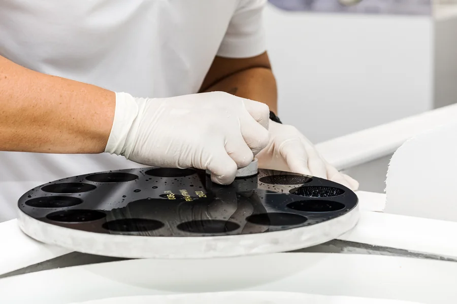
Once the ingot cools, it's sliced into individual wafers with a wire saw, then lapped and polished to remove saw damage and achieve a mirror finish. Flatness tolerances here are unforgiving. NIST researchers developing a new infrared measurement tool noted that leading-edge wafers require site flatness under 45 nanometers, a tolerance so tight that even the interferometers used to check it had to be redesigned.
That level of precision is why polishing errors, not crystal growth mistakes, cause a large share of rejected wafers industry-wide.
Two credentials separate serious silicon wafer manufacturers from the rest of the market: ISO 9001 and AS9100. ISO 9001 establishes a baseline quality management system; AS9100 builds on it with additional requirements for aerospace, defense, and other high-reliability sectors. Wafer World holds both certifications, a point covered in more detail on our page about buying silicon wafers and reflected across our silicon wafer product line.
These aren't decorative badges. They require documented process control, traceability, and regular audits, which is exactly the kind of paper trail you want behind a wafer that ends up in a satellite or a medical device.
Before you commit to a supplier, run through this checklist:
Lead times vary widely across the industry because furnace capacity, polishing equipment, and cleanroom space are fixed resources; a manufacturer running near capacity cannot compress a growth cycle to meet a rush order. Facilities that maintain in-house crystal growth, slicing, and polishing under one roof, rather than outsourcing steps to third parties, tend to offer more predictable timelines because fewer handoffs mean fewer places for a schedule to slip.
Our silicon and semiconductor wafer services page outlines how that vertical process works for custom specifications.
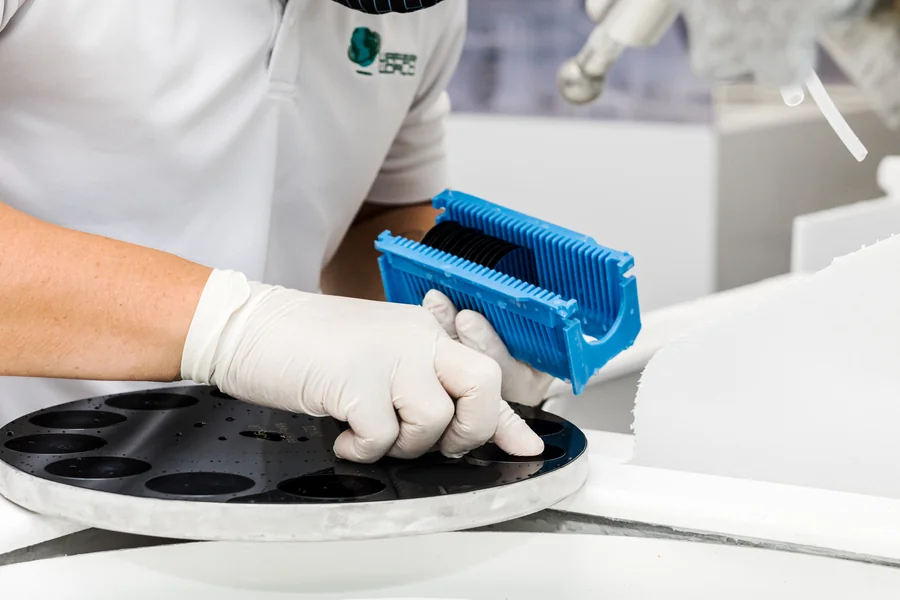
Price differences usually trace back to purity grade, ingot diameter, polishing tolerance, and whether the wafer is prime, test, or reclaimed material. Two wafers that look identical can carry very different specifications underneath.
Not necessarily. Facility size matters less than certification status, in-house process control, and documented testing. Some smaller manufacturers offer faster turnaround precisely because they carry less order backlog.
A full Czochralski growth cycle can run anywhere from several hours to a couple of days, depending on ingot diameter, which is one reason rush orders are difficult to accommodate industry-wide.
Prime wafers meet the tightest specifications for device fabrication; test-grade wafers are used for process monitoring and calibration, where minor defects don't affect the outcome.
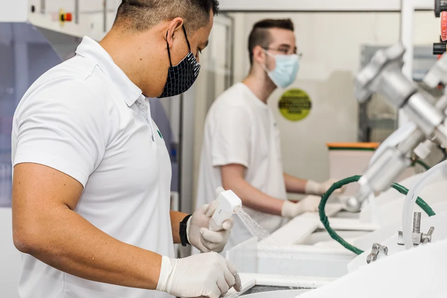
Choosing among silicon wafer manufacturers comes down to verifying the process behind the product, not just comparing price sheets. Wafer World has spent nearly three decades building that process in-house, from ingot growth through certified final inspection, and our AS9100 and ISO 9001 credentials back it up.
If you're ready to talk specs, lead times, or a custom order, contact our team, and we will help you get the right wafer the first time.




