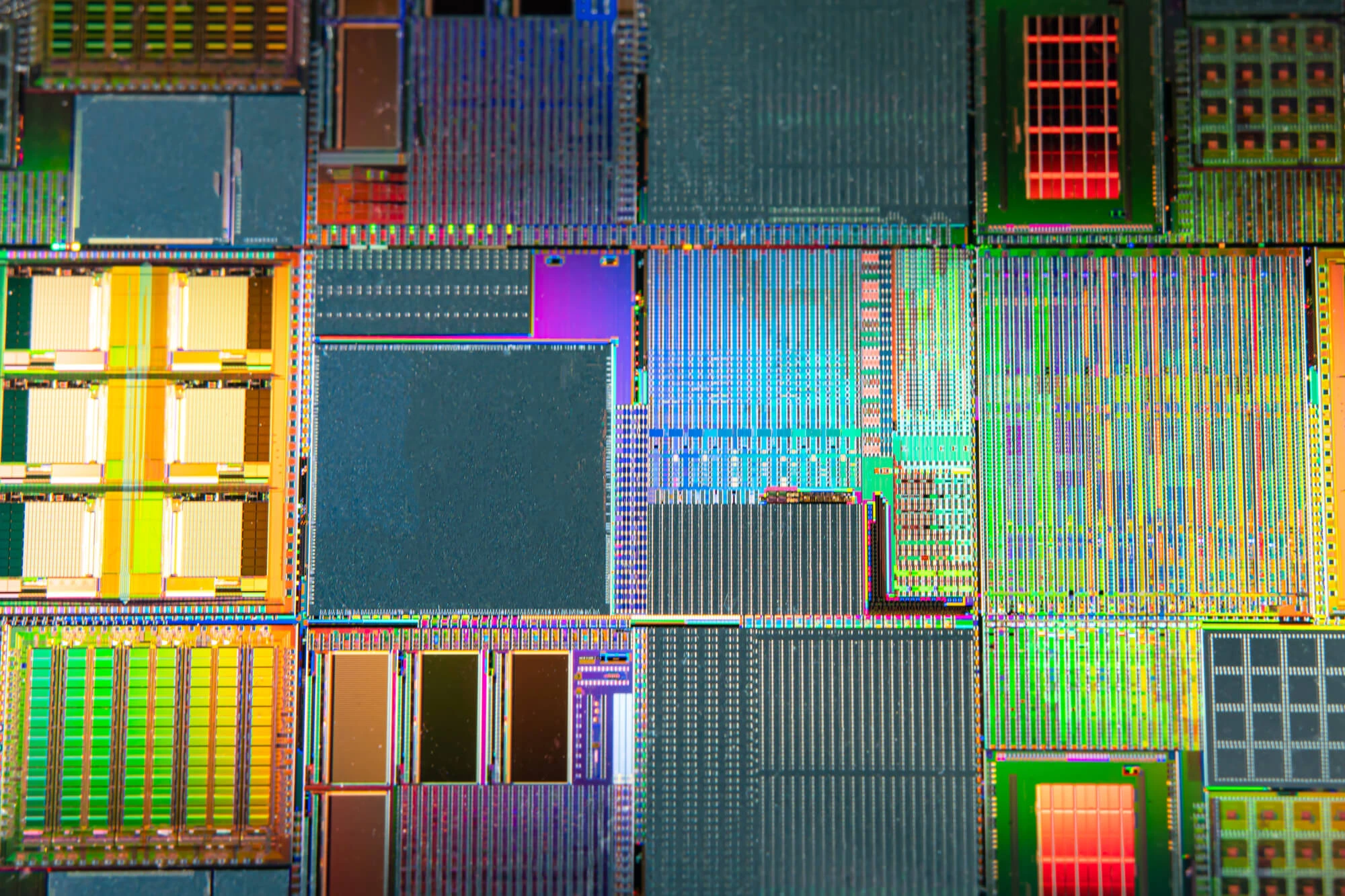
When purity and performance matter most, FZ wafers are the gold standard in semiconductor and power device manufacturing. Unlike Czochralski (CZ) silicon, the Float Zone method eliminates oxygen contamination, producing silicon with unmatched resistivity and crystal integrity.
But what exactly defines a high-quality FZ wafer?
An FZ wafer is distinguished by its exceptionally high chemical purity. Float Zone silicon typically contains less than 1 × 10¹⁶ atoms/cm³ of oxygen, which is significantly lower than that of CZ wafers.
The absence of oxygen and carbon reduces lattice defects, increasing breakdown voltage and enabling high-resistivity performance suitable for RF, power, and detector applications.
Resistivity is one of the key specifications for FZ wafers. Depending on whether or not FZ wafers are doped or undoped, their resistivity can vary greatly; this wide range makes FZ wafers highly versatile, supporting devices that require precise carrier lifetimes and low leakage currents, such as high-power diodes, MOSFETs, and particle detectors.
Common orientations include ⟨100⟩, ⟨111⟩, and ⟨110⟩, which are chosen to optimize etch rate, carrier mobility, or device symmetry.
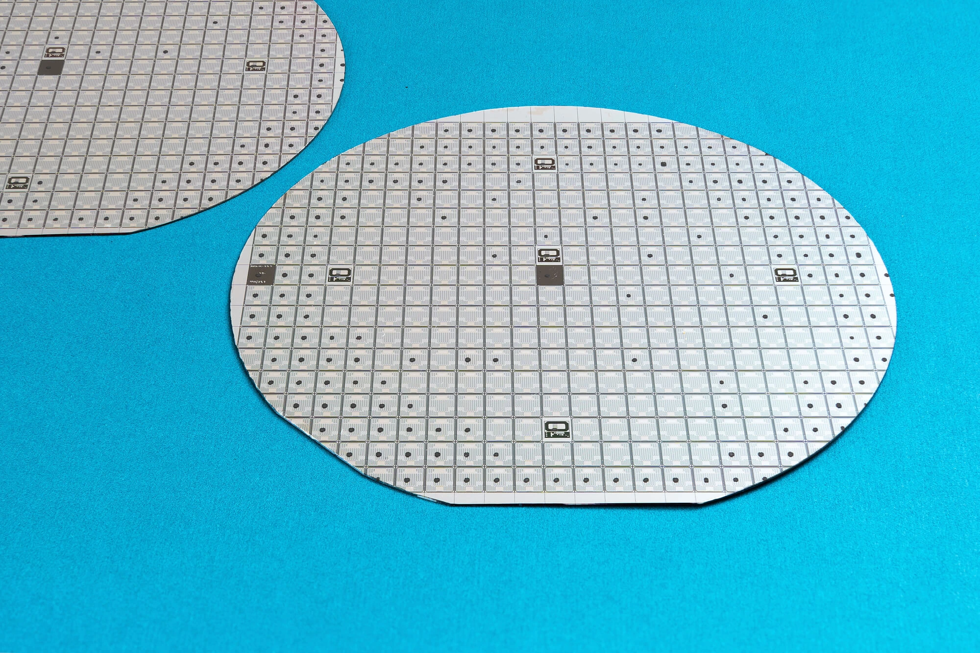
Standard diameters range from 2 inches (50.8 mm) to 8 inches (200 mm), but specialty suppliers can create custom sizes or rectangular FZ wafers for research instruments and detectors.
Float Zone processing enables precise doping control and extremely low defect densities. This uniformity results in stable electrical characteristics across the wafer, which is essential for precision analog, metrology, and photonics applications.
DSP (Double-Side Polished) surfaces are ideal for optical and MEMS applications. SSP (Single-Side Polished), on the other hand, can be used in standard device fabrication.
The typical thickness ranges from 280 to 525 µm, depending on the diameter and application.

Whether you’re designing high-voltage switches, radiation detectors, or next-gen photonic chips, understanding Float Zone wafer specs helps you select the right material for your performance goals. With purity, uniformity, and flexibility in customization, FZ wafers remain the premium choice for advanced semiconductor innovation.
Would you like to learn more about the performance of our materials? Contact Wafer World today and let’s talk!


