Selecting the right Si wafer begins with understanding its core specifications. Diameter, crystal orientation, and resistivity directly influence device design, electrical behavior, and process compatibility. Whether for research or volume production, knowing how these parameters interact helps ensure consistent semiconductor performance.

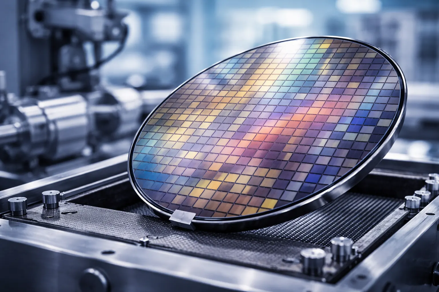
Wafer diameter determines how many devices can be fabricated per substrate. Common sizes range from 2 inches to 300 mm, with larger diameters supporting higher throughput. Uniform thickness and flatness become increasingly important as size increases. Selecting the correct diameter supports equipment compatibility and fabrication efficiency.
As device geometries shrink, surface uniformity and edge exclusion zones require tighter control. Larger substrates must meet strict tolerances to maintain yield across the entire surface.
Crystal orientation refers to the alignment of the silicon lattice, commonly <100> or <111>. Orientation affects oxidation rates, etch profiles, and carrier mobility. Choosing the appropriate orientation ensures predictable behavior during diffusion and patterning steps.
For example, <100> orientation is widely used in CMOS manufacturing due to favorable interface characteristics, while <111> may be selected for specific MEMS or power applications.
Resistivity reflects dopant concentration and determines how easily current flows through the substrate. A Si wafer with low resistivity supports high conductivity applications, while high-resistivity material is often preferred for RF or detector technologies. Engineers must match resistivity ranges to device requirements to avoid performance inconsistencies.

Selecting the correct Si wafer involves balancing diameter, orientation, and resistivity with your technical objectives. At Wafer World, we work with research institutions and manufacturers to provide specification-driven wafer solutions. Contact us today to discuss your requirements and connect with our team for expert guidance.


