September 8, 2025
Shop NowIon implantation doping is a crucial stage in the production of semiconductors. This technique involves purposefully adding atoms to silicon wafers that have conduction-enabling impurities. After you buy a silicon wafer, ion implantation is a complex procedure that requires top-notch equipment and high-quality raw materials.
However, as the complexity of semiconductor chips has increased, so has the number of ion implants needed—and the intricacies of this procedure.
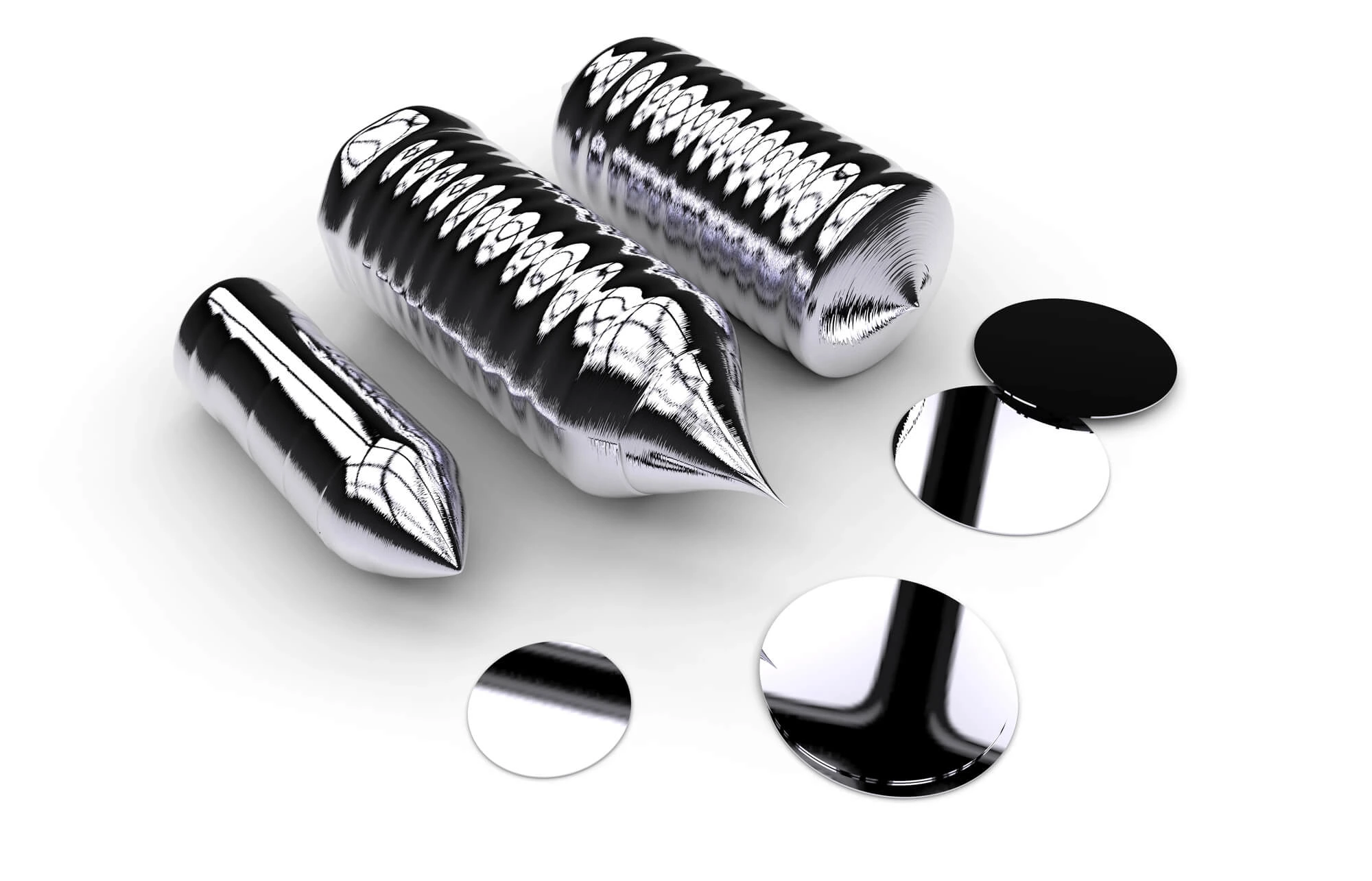
Ionization, or ion implantation, is the process of forming ions from an atom or a molecule, either by the gain or loss of electrons. An anion is a negatively charged ion formed by the gain of electrons by an atom or a molecule. Similarly, a positively charged ion formed by losing electrons from an atom or a molecule is called a cation.
Modifying a material’s surface by implanting ions of one material into another causes a change in physical and chemical properties. For that reason, silicon ion implantation has become a critical process in wafer manufacturing.
For manufacturing semiconductors, fabs introduce dopant ions—such as boron, phosphorus, or arsenic—into a silicon wafer and modify its electrical properties. This technique allows for precise control over doping concentration, depth, and uniformity, making it a preferred method over traditional diffusion techniques.
Unlike thermal diffusion, which relies on high-temperature environments, ion implantation uses an accelerated ion beam to physically embed ions into the silicon substrate. This provides better spatial resolution and greater consistency across the wafer surface, essential for producing high-performance integrated circuits.
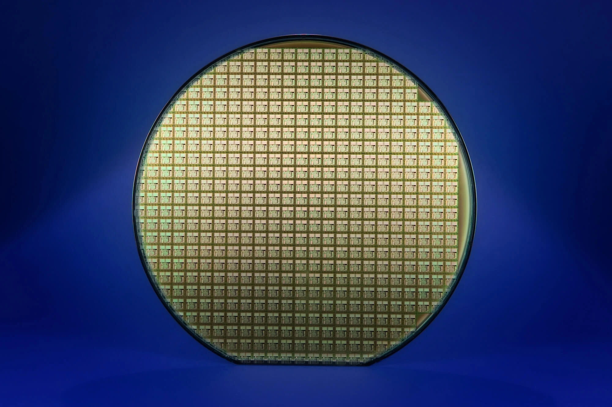
Silicon remains the dominant semiconductor material due to its abundance, cost-effectiveness, and well-understood properties. Its crystalline structure is ideal for ion implantation because it allows dopant ions to be precisely introduced without compromising the substrate’s integrity.
This process results in minimal contamination and high purity, and it's compatible with modern photolithography techniques. Moreover, silicon ion implantation can be customized for diverse semiconductor needs, which is why it is also scalable for high-volume production.
Ion implantation into silicon enables:
The process generally follows these steps:
1. Ion Generation: A source gas (like arsine or phosphine) is ionized in a plasma chamber.
2. Acceleration: Ions are accelerated by an electric field to gain kinetic energy.
3. Mass Separation: Magnetic fields separate the desired ions from contaminants.
4. Targeting: The ion beam is directed at the silicon wafer in a vacuum environment.
5. Implantation: Ions penetrate the silicon surface to the desired depth.
6. Annealing: Post-implantation heating repairs crystal damage and activates dopants.
This control and repeatability level makes ion implantation a cornerstone of modern semiconductor fabrication.
Ion implantation techniques are essential in semiconductor manufacturing, particularly for doping silicon wafers. Some methods include:
This variation allows for batch processing of wafers and is suitable for high-volume manufacturing. In PIII, the wafer is immersed in plasma, and ions are accelerated by applying a high-voltage pulse to the wafer itself. It eliminates the need for beam scanning and reduces system complexity.
Low-energy implantation is used for shallow junctions, typical in modern CMOS devices. High-energy implantation is applied when deeper penetration is needed, such as in power semiconductors.
While fast neutron irradiation introduces defects and dopants through exposure to high-energy neutrons, ion implantation offers superior precision and is less damaging to wafer integrity.
Neutron techniques are used more in specialized or experimental contexts, while ion implantation remains the standard for mainstream semiconductor production.
Ion implantation requires specialized, high-precision equipment that handles cleanroom conditions and tight specifications. Key components include:
Manufacturers often invest heavily in these systems or partner with foundries that offer ion implantation as a service.
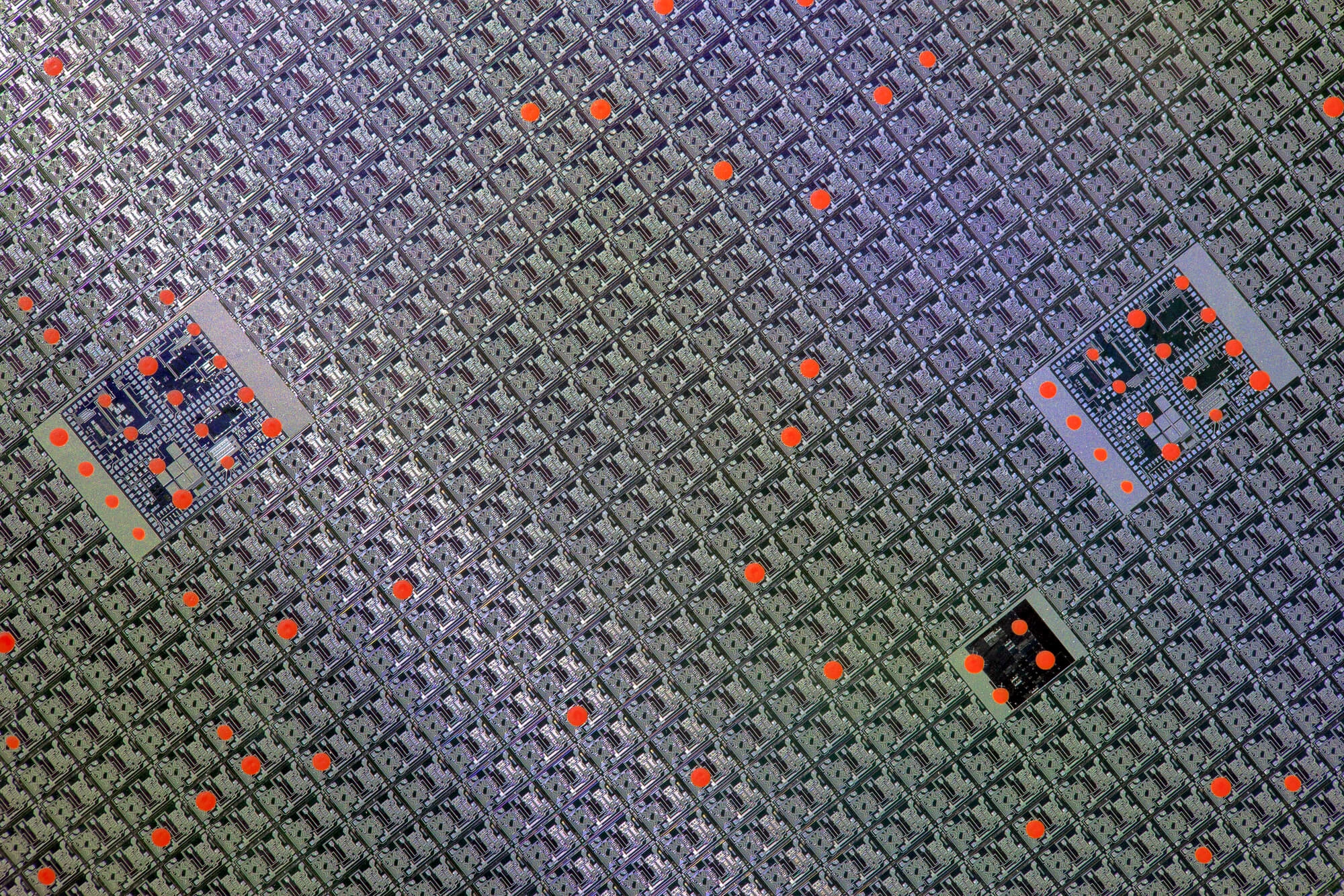
Ion implantation is used across various semiconductor applications, including:
As device geometries shrink and performance demands rise, implantation precision becomes even more crucial.
While ion implantation offers precision and control, it also presents technical challenges. When high-energy ions disrupt the silicon crystal structure, lattice damage can occur, requiring precise annealing to repair defects and activate dopants.
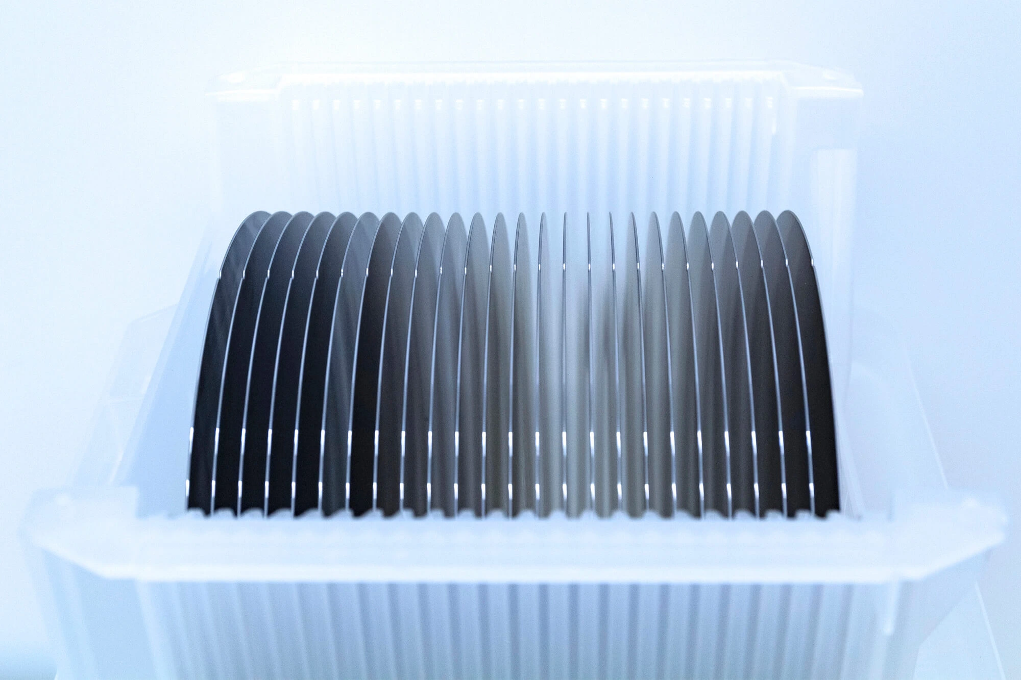
Moreover, achieving ultra-shallow junctions without diffusion is increasingly difficult as devices shrink, and dose uniformity across large wafers remains a constant manufacturing concern. Additionally, maintaining cleanroom conditions and tool calibration is essential to avoid contamination and ensure repeatability in high-volume production.
When you’re ready to buy silicon wafers for ion implantation, consider the following:
Partnering with a trusted wafer supplier ensures your implantation process is efficient, defect-free, and scalable.
Silicon ion implantation is vital in semiconductor manufacturing, enabling precise control over electrical properties in modern devices. As technology advances and devices become smaller and more complex, high-precision doping through ion implantation will remain central to innovation.
Whether you're a researcher, manufacturer, or sourcing manager, understanding the intricacies of ion implantation and choosing the right silicon wafers can make all the difference in device performance and yield. If you want to check whether our wafers are right for your project, contact Wafer World today!


