September 1, 2025
Shop NowIn the world of silicon manufacturing, the precision and performance of every thin film layer matter. Whether you're building transistors, MEMS devices, or optical coatings, choosing the right deposition technique can significantly impact yield, reliability, and device performance.
Physical Vapor Deposition (PVD), Chemical Vapor Deposition (CVD), and Atomic Layer Deposition (ALD) are three of the most widely used methods during this stage. While all of them work to deposit thin films onto substrates, they differ significantly in mechanism, control, film quality, and application scope. You can choose the right technique for your specific application by understanding these differences.
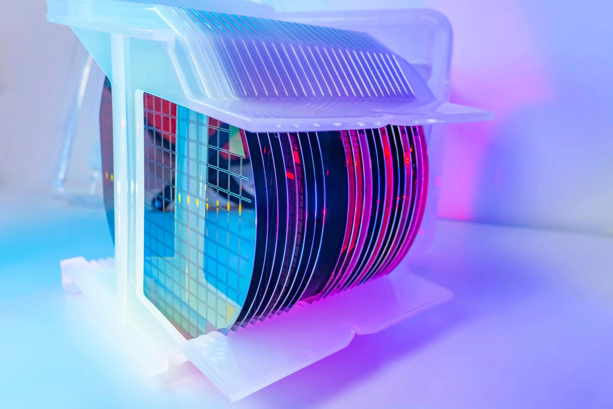
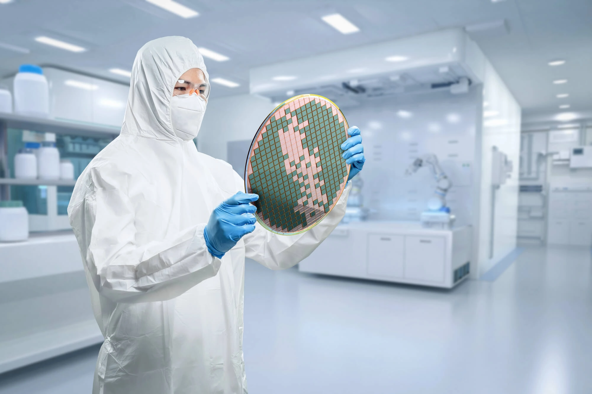
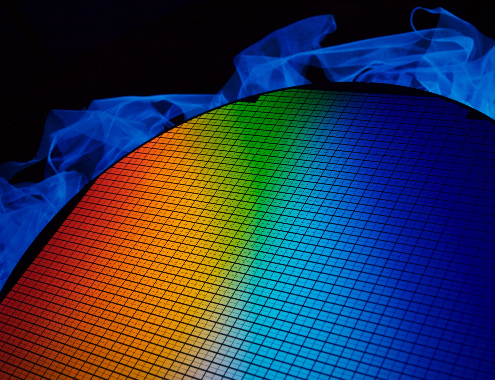
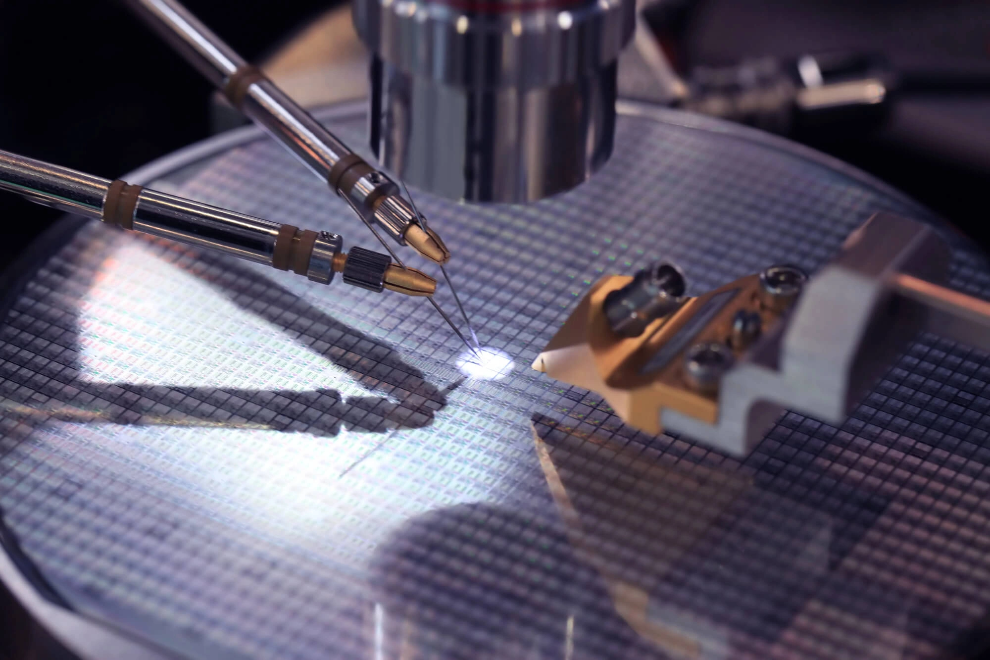
Thin-film deposition is a critical step in semiconductor fabrication. It involves depositing ultra-thin material layers—sometimes only a few atoms thick—onto a silicon wafer. These layers are conductors, insulators, barriers, or functional surfaces in microchips and sensors.
There are three main deposition methods:
Each has its advantages depending on the end product's material, feature size, and functional requirements.
PVD is a physical process where material is vaporized from a solid source and then condensed onto the target wafer. There are two main types of PVD:
Common applications include metal interconnects (e.g., Al, Cu, TiN), reflective coatings in optics, and wear-resistant layers on tools.
PVD has noticeable advantages, such as high deposition rates and a relatively low cost. These, combined with the fact that it can be performed with a wide range of materials (metals, alloys, ceramics, and more), make it a scalable technique.
It’s particularly good for larger feature sizes and robust coatings.
On the other hand, some of PVD's disadvantages include poor step coverage on high aspect ratio structures, difficulty controlling film thickness at atomic scales, and the line-of-sight process, which can lead to shadowing effects.
Chemical Vapor Deposition (CVD) is a widely used thin-film deposition process in semiconductor and silicon manufacturing. In this process, a solid material is deposited from a gas-phase chemical reaction onto a substrate. CVD is critical in forming dielectric layers, diffusion barriers, and even conductive films on silicon wafers.
Unlike PVD, a physical process, CVD relies on chemical reactions to form high-purity, conformal coatings—making it a key technique in producing microelectronics, solar cells, and MEMs.
CVD can deposit films with uniform thickness even on complex 3D geometries, similar to ALD. Silicon dioxide (SiO₂), silicon nitride (Si₃N₄), polysilicon, tungsten (W), and many other materials can be deposited via CVD.
The chemical reactions also produce dense, low-defect coatings suitable for electronic-grade applications.
Many CVD processes require 400–900°C, which may not be compatible with all substrates or device layers. Some gases used in this process, like silane, ammonia, and hydrogen chloride, are also hazardous, requiring specialized gas handling and exhaust systems.
Reactions must be carefully controlled to avoid particle formation or incomplete deposition.
ALD is a chemical vapor deposition technique that deposits thin films one atomic layer at a time. It uses sequential, self-limiting reactions between gaseous precursors and the substrate surface.
Each cycle deposits a sub-monolayer of material, and repeating the cycle builds the film to the desired thickness.
Common applications for this method include high-k dielectric layers in CMOS (e.g., HfO₂, Al₂O₃), barrier layers in 3D NAND and DRAM, coatings for MEMS and nanodevices.
ALD allows for atomic-level control of thickness and composition. It is excellent step coverage, even on complex 3D geometries. The ultra-conformal coatings are ideal for nanoscale devices. Additionally, this method offers highly uniform and pinhole-free films.
The biggest downside of ALD is that it offers slower deposition rates compared to PVD. Moreover, process control is more complex, which results in higher equipment and process costs.
ALD is also limited to specific material systems.
PVD is the go-to method when:
You should consider using CVD when:
ALD shines in applications where:
In advanced silicon manufacturing, it’s not always a matter of PVD versus ALD versus CVD. Often, these techniques are used together within the same process stack.
For example:
This hybrid strategy allows engineers to balance cost, speed, and precision—crucial in today’s high-density chips and multilayer architectures.
Choosing between Physical Vapor Deposition (PVD), Chemical Vapor Deposition (CVD), and Atomic Layer Deposition (ALD) depends on your specific application, required film properties, and manufacturing constraints.
While PVD remains ideal for metallic layers and ALD is best for ultra-thin, precise coatings, CVD bridges the gap—delivering excellent film quality and geometry coverage for various materials and applications in the semiconductor world. Do you have any doubts? Contact Wafer World for more information!


