Silicon manufacturing plays a central role in enabling reliable power devices and high-performance IC applications. From raw material refinement to polished wafers, every step influences electrical characteristics, yield, and long-term device stability.
The process begins with high-purity polysilicon. Using methods such as the Czochralski process and Float-Zone refining, single-crystal ingots are grown with controlled resistivity and orientation.
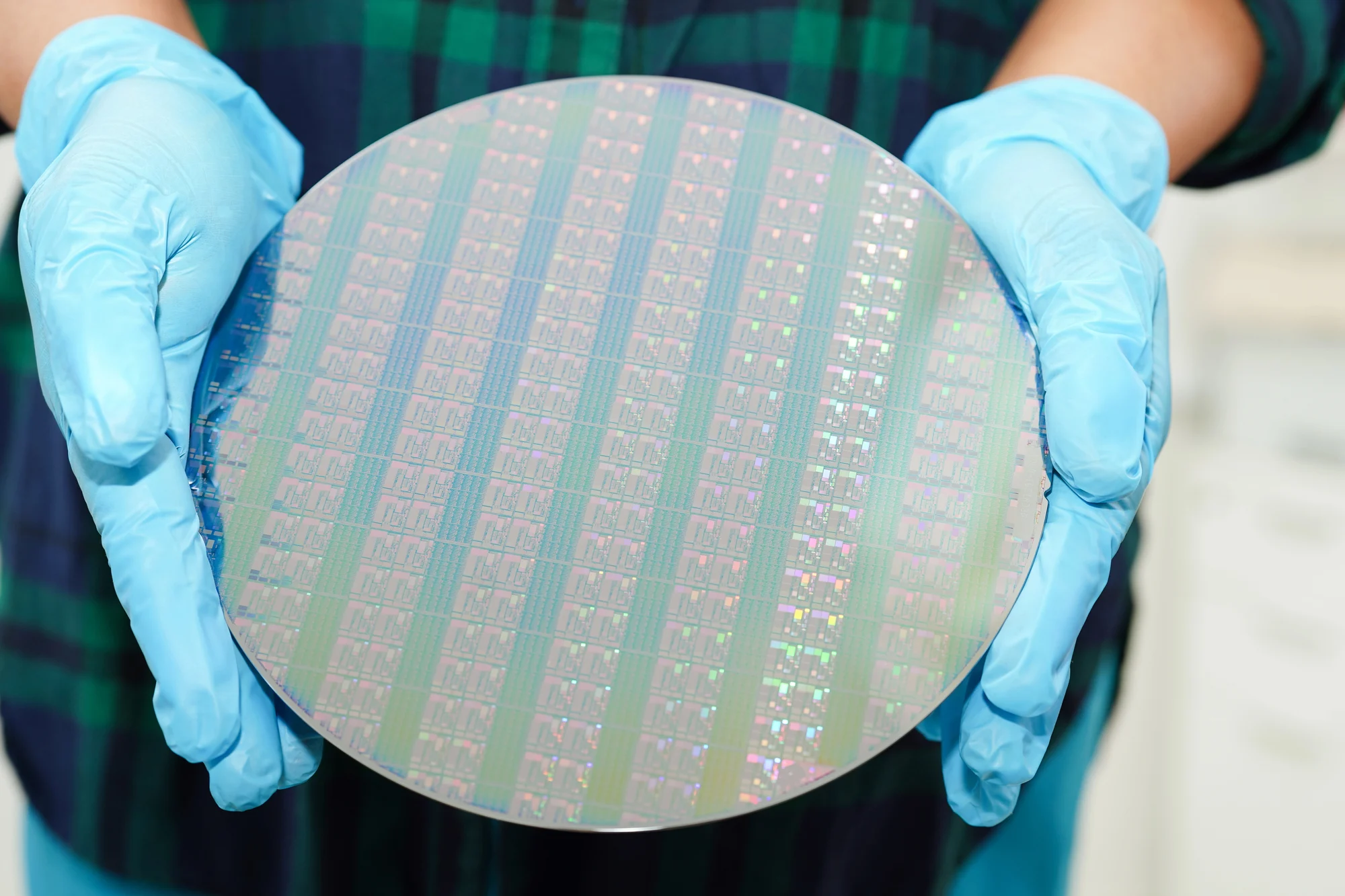
These ingots are then sliced into wafers, lapped, etched, and polished to achieve tight thickness tolerances and flatness requirements.
Czochralski silicon is widely used for IC production due to scalability and cost efficiency. Float Zone silicon, known for its high purity and low oxygen content, is often selected for demanding power applications where performance under high voltage is critical.
In silicon manufacturing, parameters such as resistivity range, crystal orientation, oxygen content, and surface quality directly impact device fabrication. Power devices typically require specific resistivity profiles to manage current flow and breakdown voltage.
IC applications demand uniformity across the wafer to maintain circuit integrity at smaller nodes.
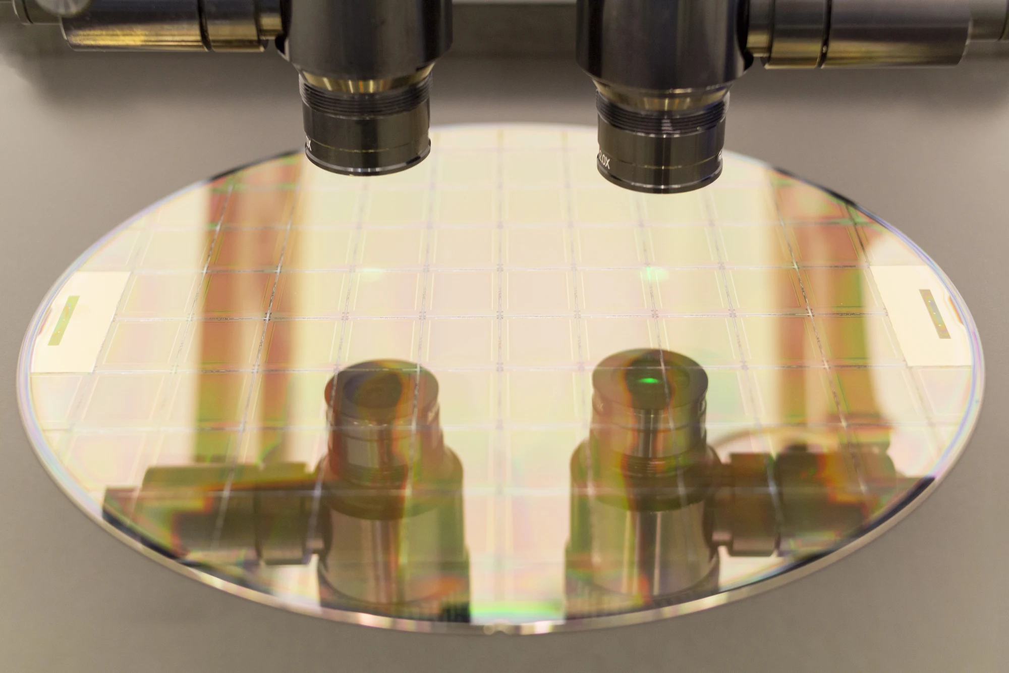
Advanced inspection methods verify total thickness variation, flatness, and surface defects. These quality checks help ensure compatibility with downstream processes like epitaxy, oxidation, and lithography.
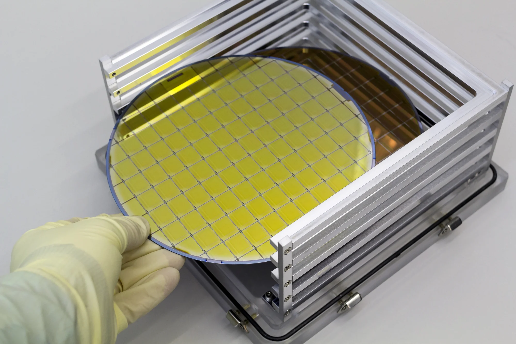
Reliable silicon manufacturing also depends on consistent sourcing and customization. Wafer diameter, doping type, and reclaim options may vary depending on R&D or production-scale requirements.
For teams seeking dependable silicon manufacturing support for power devices and IC development, working with an experienced wafer supplier can streamline specifications, logistics, and quality expectations.
At Wafer World, we collaborate closely with engineers and procurement teams to align wafer characteristics with application goals. Connect with us to discuss your project requirements.


