
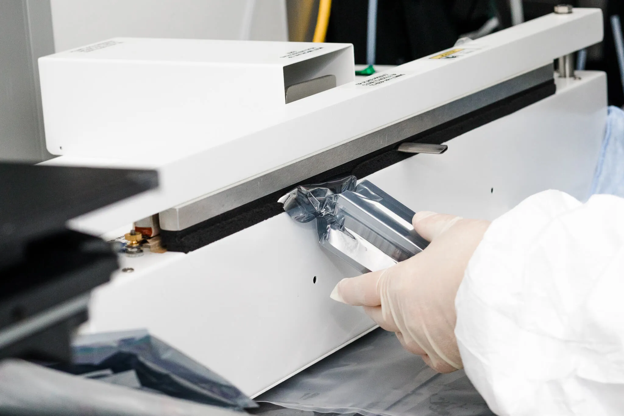
Wafers are the building blocks of all of our technology, as they form the foundational substrate upon which integrated circuits (ICs) are built. For that reason, ensuring the surface quality of every single Si wafer is critical.
Defects on wafer surfaces—such as particles, scratches, pits, and microcracks—can lead to performance issues, yield loss, and reliability failures, affecting a product's performance and reducing durability. That's why wafer manufacturers employ various surface inspection methods to maintain stringent quality standards. In this article, we'll explore some of them.
Effective surface inspection allows manufacturers to take corrective actions before defects propagate through the production line. A semiconductor wafer's quality directly impacts the final devices' long-term dependability and manufacturing yield.
Crystal growth, wafer slicing, polishing, cleaning, handling, and transportation are some of the processes that can result in surface flaws. Moreover, flaws on wafers can look very different: They can be caused by unwanted particles, such as dust, residue, or foreign materials, getting deposited on the wafer surface.
They can also appear as scratches on the wafer’s surface caused by mechanical contact during processing. Whatever it is, flaws carry problems down the production line, so identifying them early on is crucial to:
Nowadays, various surface inspection methods are available for semiconductor fabs to analyze the quality of wafers—often combined to ensure the best possible results.
Some of these include:
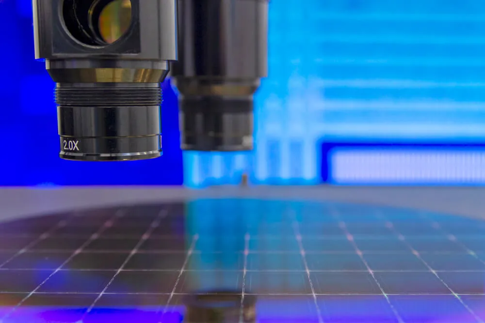
Optical inspection illuminates the wafer surface using visible or ultraviolet (UV) light, then looks for anomalies based on variations in contrast, light scattering, or reflection. It’s a fast, non-contact inspection method that can detect particles, scratches, and pattern defects across full wafers. Additionally, it's compatible with automated inspection systems.
However, in contrast to other techniques, optical inspection is less sensitive to subsurface flaws and provides less resolution than electron-based techniques.
There are various types of optical inspections:
During laser scanning inspection, a focused laser beam scans the wafer surface, and photodetectors capture the reflected or scattered light to identify defects.
This method measures wafer flatness and surface roughness and offers high sensitivity to minute features. In fact, laser scanning can detect particles as small as 20 nm. Still, it can scan large areas rapidly, avoiding bottlenecks in the production process.
It has two working modes:
One limitation of the method is that it may require calibration for different surface materials. Additionally, its effectiveness for deep subsurface defects is limited.
SEM uses a focused beam of electrons to scan the wafer surface, producing high-resolution images based on electron-surface interactions.
This allows Si wafer manufacturers to identify very small defects (in the nanometer scale) and conduct an in-depth analysis of defect morphology. Moreover, SEM surface inspection offers an extremely high spatial resolution and is capable of conducting 3D topographical analysis.
The downside, though, is that this method offers considerably low throughput. For that reason, it's typically only used for defect review, not in-line inspection. Additionally, it requires a vacuum environment and careful sample preparation, and it is incompatible with certain industrial processes.
AFM uses a sharp probe that scans the surface at the nanoscale, measuring forces between the tip and surface to generate a topographic map. It measures surface roughness, scratches, or pits. Additionally, it allows for nanoscale defect characterization in ultra-high resolution, reaching even sub-nanometers.
AFM surface inspection works in ambient or controlled environments, but scan areas must be limited. This can slow scan speed and make it unsuitable for whole-wafer inspection.
IR inspection allows for identifying internal cracks, voids, or dislocations. It’s used primarily on unpatterned wafers. The principle is that IR light penetrates silicon wafers and reflects off buried layers or defects, enabling the detection of subsurface irregularities.
This method is nondestructive and noncontact and detects subsurface issues missed by optical techniques. Non-destructive testing (NDT) means that you can examine and evaluate materials, components, or systems without causing damage or altering their properties
Its downsides are that it's less effective on patterned wafers and offers lower resolution compared to other inspection techniques, such as SEM or AFM.
X-ray inspection uses high-energy radiation to penetrate the wafer and detect internal defects based on density or compositional differences. While its effectiveness is limited to surface-level defects, this non-destructive method allows the imaging of internal structures.
This makes it effective for identifying defects in advanced packaging or 3D ICs. Moreover, it analyzes TSVs (Through-Silicon Vias) and bonding layers. For that reason, the equipment cost and complexity are often worth the investment.
.webp)
Modern semiconductor fabrication facilities incorporate a variety of surface inspection techniques into in-line monitoring systems and automated inspection tools. These systems gather defect data in real time, which is fed into machine learning algorithms and statistical process control (SPC) for process optimization and defect prediction.
Moreover, AI technologies are now being used to recognize patterns in defects and surface anomalies and prevent them in the future to reduce costs.
Surface inspection is a key component of wafer quality control in semiconductor production. Ensuring the detection of even the smallest surface and subsurface flaws becomes crucial as devices grow to smaller geometries and more intricate structures.
Some surface inspection methods offer quick, in-line control capabilities, while others provide high-resolution insight into defect mechanisms. Understanding how to combine these two faculties in synergy is crucial for wafer manufacturers to maintain high yields. If you’d like to learn more about our surface inspection methods, contact Wafer World today!


