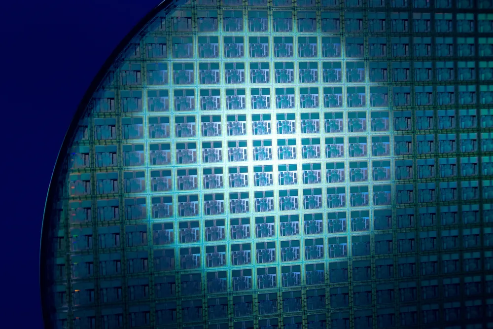
Direct bonding, or fusion bonding, describes a wafer bonding process without any additional intermediate layers. The bonding process is based on chemical bonds between two surfaces of any material. These requirements are specified for the wafer surface as sufficiently clean, flat and smooth. Let’s take a deeper look at direct wafer bonding and how it pertains to silicon prices.
Direct bonding of surfaces has been used since the early 1960s and has strongly influenced the engineering of many innovative substrates and structures. Philips Labs developed one of the first applications: direct bonding of mirrors for flat mirror gas laser structures. The most well-known application is the mass production of silicon on insulator bonded structures. Advances in direct wafer bonding have lead to it being used in new applications such as microelectronics, microtechnologies, sensors, MEMs, optical devices, biotechnologies and 3D integration.
Direct wafer bonding consists of connecting two wafer surfaces without any adhesive or additional materials to promote the adhesion between the two surfaces. It allows different materials to be stacked together without concern for the crystalline relationship between them. Direct bonding has been developed as an alternative route to many other bonding processes, such as anodic bonding, thermo-compression bonding, eutectic bonding, glass fitting, and polymer adhesive bonding.
Direct bonding is commonly performed in a clean room with hydrophilic or hydrophobic surfaces. Smooth surfaces and suitable surface bonds are needed to enable direct bonding.
At Wafer World, we offer direct wafer bonding at competitive prices. Contact us today to learn more about the wafers and prices that we offer.


